

SEGGER Microcontroller GmbH
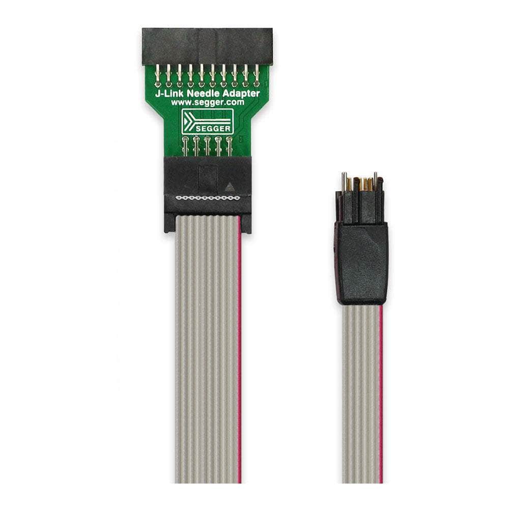
SEGGER 10-Pin Needle Adapter for J-Link Debug Programming
SEGGER 10-Pin Needle Adapter for J-Link Debug Programming
SKU: 8.06.04
Couldn't load pickup availability
Key Features
Overview
The SEGGER 10-Pin Needle Adapter represents a sophisticated solution for embedded developers seeking to eliminate bulky programming headers whilst maintaining full debug capabilities. This precision-engineered adapter bridges the gap between SEGGER's standard 20-pin debug interface and a minimal 10-pin needle footprint on your target PCB.
Unlike traditional headers that consume valuable PCB real estate and add component costs, this needle adapter contacts directly with copper pads through high-reliability spring pins. The innovative three-pin positioning system prevents incorrect connections whilst the robust spring contacts withstand over 100,000 programming cycles.
Engineers choose this solution for space-constrained designs, high-volume production runs, and anywhere connector costs impact project viability. The adapter supports both JTAG and SWD protocols with optional target power delivery, making it suitable for everything from initial prototype bring-up to final production programming. Compatible with the complete range of SEGGER J-Link debug probes and Flasher production tools, this adapter integrates seamlessly into existing development workflows.
Downloads
Why Engineers Choose The SEGGER 10-Pin Needle Adapter for J-Link Debug Programming
Eliminate Header Costs
Space-Constrained Designs
Production Reliability
Advanced Needle Adapter for Connector-Free Programming
The SEGGER 10-Pin Needle Adapter transforms how engineers connect J-Link and Flasher debug probes to target PCBs. This precision adapter eliminates the need for mounted connectors on your circuit boards whilst providing reliable spring-pin contact to a specialised footprint pattern.
Foolproof Connection Design
Three strategically positioned locating pins ensure the adapter can only connect in the correct orientation, preventing costly connection errors during development and production programming.
Technical Specifications
| Input Connector | 20-pin 0.1" (2.54mm) standard JTAG/SWD |
|---|---|
| Output Pattern | 10-pin 0.05" (1.27mm) needle pattern |
| Spring Pins | High-reliability, >100,000 cycle rating |
| PCB Footprint | Minimal space requirement with tri-pin keying |
| Target Power | Optional 5V supply via pin 9 (300mA max) |
Signal Mapping & Pinout
The adapter provides full JTAG and SWD signal access including:
- JTAG Signals: TCK, TDI, TDO, TMS, TRST
- SWD Signals: SWCLK, SWDIO, SWO
- Control: RESET, VTref, GND
- Power: 5V target supply (optional)
PCB Layout Requirements
Pad Specifications: - Contact pads: 0.8mm diameter minimum - Positioning holes: 0.7mm diameter - Solder mask: Must be clear of contact pads - No solder paste on needle contact areas - 0.5mm clearance from other tracesCompatible Debug Probes
Works seamlessly with all SEGGER debug tools including J-Link BASE, PLUS, PRO, ULTRA+, EDU, and Flasher series. The 20-pin standard interface ensures universal compatibility across the SEGGER ecosystem.
| General Information | |
|---|---|
Product Type |
Adapter
|
Part Number (SKU) |
8.06.04
|
Manufacturer |
|
| Physical and Mechanical | |
Weight |
0.02 kg
|
| Other | |
EAN |
5055383614448
|
Questions and Answers
-
Is This Adapter Compatible with Third-Party Debug Probes?
The adapter uses a Tag-Connect-style spring-pin footprint (SEGGER's footprint drawing carries the Tag-Connect patent notice) with SEGGER's own 10-pin signal assignment. SEGGER lists J-Link and Flasher models as suitable products and does not state whether other debug probes are supported. If you are designing for a different probe, see Tag-Connect TC2050 solutions.
-
Can I Use This for SWD Debugging Without JTAG Signals?
Yes. The adapter supports both JTAG and SWD through the same footprint. SWD uses the SWCLK and SWDIO signals mapped to the needle pattern.
-
What Happens If I Need to Modify the Cable or Connector?
For custom modifications or different cable lengths, contact SEGGER directly. For custom pin mapping, use the 50-mil 10-pin patch adapter, which allows custom connections and wiring.
-
How Do I Ensure Reliable Contact During Automated Testing?
SEGGER's design holds the adapter in place with latching legs that clip into holes in the PCB, with finger access to the leg tabs, rather than relying on applied pressure. Follow SEGGER's footprint drawing for the leg latch holes and contact pads, and keep solder paste off the contact pads.
-
Does the Adapter Work with All SEGGER Debug Software?
Yes. As a passive adapter it is transparent to debug software, so SEGGER tools, including J-Link Commander and the Ozone debugger, and third-party IDEs should work without modification.
-
What's the Difference Between This and the 6-Pin Needle Adapter?
The 10-pin version provides full JTAG (TDI, TDO, TCK, TMS) plus optional target power. The 6-pin variant supports SWD debugging only. Choose 10-pin for maximum compatibility.
-
Can I Power My Target Board Through This Adapter?
Yes, the 5V-Supply needle (pin 5) provides 5V at up to 300mA from a J-Link for target power, so you don't need a separate power supply during programming and debugging.
-
How Does the Positioning System Prevent Incorrect Connections?
Three precision-positioned locating pins mechanically key the adapter to your PCB footprint. It physically cannot connect incorrectly, which prevents damage from reverse or offset connections.
-
What PCB Layout Rules Must I Follow for the Needle Footprint?
Follow these rules:
- Contact pads: 0.79mm (0.031in) diameter
- Alignment pin holes: 0.99mm (0.039in) diameter, non-plated
- Leg latch holes: 2.37mm (0.0935in) diameter, non-plated
- Keep 0.5mm clearance from other traces
- Never apply solder paste to contact areas
-
How Many Programming Cycles Can I Expect From the Spring Pins?
SEGGER does not publish a connection-cycle rating for the spring pins, so we cannot quote one. SEGGER describes them as high-reliability spring pins.


No questions match your search.