


SEGGER Microcontroller GmbH
SEGGER J-Link 6-Pin Needle Adapter (8.06.16)
SEGGER J-Link 6-Pin Needle Adapter (8.06.16)
SKU: 8.06.16
Couldn't load pickup availability
Key Features
Overview
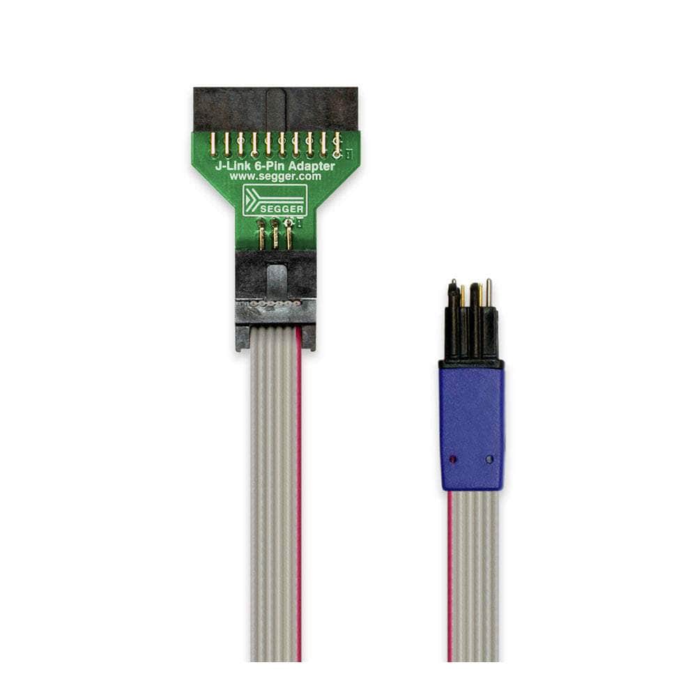
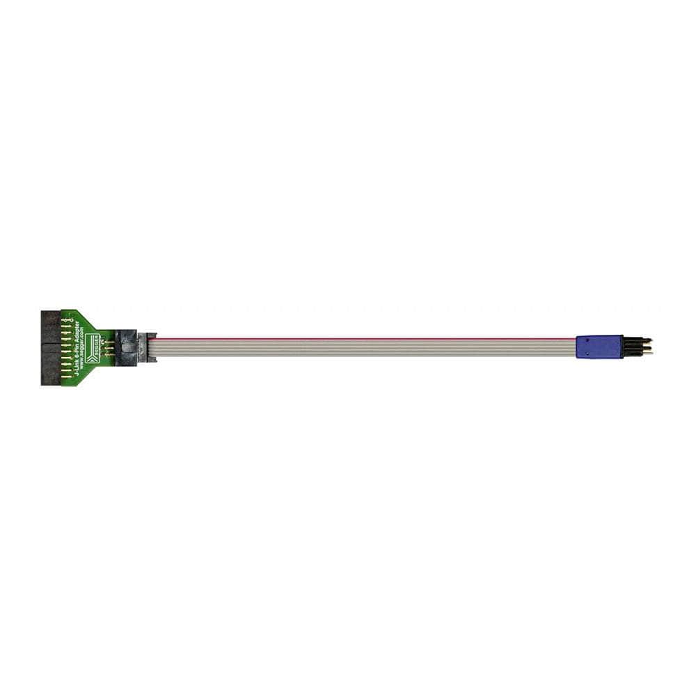
SEGGER 8.06.16 – J-Link 6-Pin Needle Adapter connects a J-Link or SEGGER Flasher to a PCB that omits a mating connector or header. It adapts from the standard 20-pin 0.1″ J-Link/JTAG connector to a compact 6-pin spring-needle pattern intended for SWD-based bring-up and production programming. A tri-pin locating pattern ensures correct orientation, while high-reliability spring pins provide stable contact during test and programming.
This 6-pin variant targets SWD; if full JTAG or target-power pin support is required, consider the SEGGER 10-Pin Needle Adapter (8.06.04). For alternative compact connectors (e.g., Cortex-M 10-pin 0.05″), see the 50-Mil 10-Pin Patch Adapter, and for general J-Link probes visit J-Link BASE Compact.
Engineers choose the needle approach to save PCB area and remove BoM and assembly cost associated with fitted headers, particularly in space-constrained or high-volume designs. The footprint and pinout are widely documented, simplifying PCB library creation and production use.
What to know: Six pins support SWDIO, SWCLK, RESET, SWO (optional), VTref and GND; for JTAG (TMS/TCK/TDI/TDO) use the 10-pin needle adapter.
Downloads
Why Engineers Choose The SEGGER J-Link 6-Pin Needle Adapter (8.06.16)
Eliminate Headers On Production PCBs
Orientation-Safe, Repeatable Contact
Fits Existing J-Link Workflows
| General Information | |
|---|---|
Product Type |
Adapter
|
Part Number (SKU) |
8.06.16
|
Manufacturer |
|
| Physical and Mechanical | |
Weight |
0.02 kg
|
| Other | |
EAN |
5055383614318
|
Frequently Asked Questions
Have a Question?
-
What if I need a different connector standard later on?
SEGGER provides adapters such as the 50-Mil 10-Pin Patch Adapter and the Target Supply Adapter to cover other scenarios.
-
Any workflow tips for first bring-up?
Follow SEGGER SWD pin guidance (VTref, RESET handling, optional SWO). Verify pull-ups/downs per device vendor before first connection.
-
How does this compare to more expensive fixtures?
Versus custom bed-of-nails fixtures, needle adapters offer much lower NRE and faster setup while still giving repeatable contact for programming.
-
What PCB footprint size should I plan for?
Use SEGGER’s published pad pattern from the datasheet; the footprint is smaller than a fitted header, aiding dense layouts.
-
Will it work with J-Link BASE/PLUS/PRO and SEGGER Flashers?
Yes—designed for J-Link and Flasher families via the 20-pin 0.1″ connector. See also the J-Link BASE Compact.
-
Is this the same as Tag-Connect?
It’s a similar “spring-pin to pad” concept. SEGGER notes its needle pinout is based on Tag-Connect but not identical; the 10-pin variant includes a 5 V supply pin.
-
How does it ensure correct orientation?
A three-pin locating pattern keys the adapter so it only mates one way. This reduces operator error and rework.
-
Does it supply power to the target?
The 6-pin version is intended for SWD signalling. If you need JTAG and the 5 V target-power pin via needle connection, use the 10-pin needle adapter (8.06.04).
-
Which signals are available on the 6-pin footprint?
VTref, SWDIO, SWCLK, RESET, GND and optional SWO for trace/printf. For JTAG signals, use the 10-pin version.
-
What problem does the 6-pin needle adapter solve?
It enables SWD debug/programming on boards without connectors, reducing BoM and PCB area while preserving J-Link workflows.