
Flash Memory Buses: Quad and Octal SPI, HyperBus and NAND
Firmware, boot images and data live in flash, and the bus to that flash decides how fast a system boots and how it fails. Small systems use SPI NOR flash on one, two, four or eight data lines; larger ones add SPI NAND, HyperBus memories or parallel ONFI NAND. A logic analyser with the matching decoder shows each command, address and data burst, and a flash programmer or SPI host adapter lets you read or reprogram the part to compare.
Interfaces Compared
| Interface | Data Lines | Typical Peak Rate | Typical Use |
|---|---|---|---|
| SPI NOR (single, dual, quad) | 1, 2 or 4 | Up to about 66 MB/s (quad at 133 MHz) | Boot and firmware storage on MCUs and SoCs |
| Octal SPI / xSPI | 8, often DDR | Up to 400 MB/s (200 MHz DDR) | Execute-in-place and fast boot on larger SoCs |
| SPI NAND | 1, 2 or 4 | Tens of MB/s | Low-cost bulk storage in routers and IoT devices |
| HyperBus | 8, DDR | Up to 400 MB/s (200 MHz) | HyperFlash and HyperRAM on automotive and industrial MCUs |
| Parallel NAND (ONFI) | 8 (or 16) | From tens of MB/s (asynchronous) to over 1 GB/s (ONFI NV-DDR3 and NV-LPDDR4) | High-capacity storage in older SoCs and SSD controllers |
Quad and Octal SPI NOR
A serial NOR transaction is a command byte, an address (three bytes, or four for parts over 128 Mbit), optional mode bits and dummy clocks, then data. Which of those phases run on 1, 2, 4 or 8 lines is set by the command: for example 0Bh (fast read) is all single line, while EBh (quad I/O read) sends the address and data on four lines. Reading SFDP (command 5Ah) returns a JEDEC-standard table of the part's commands, sizes and dummy cycles, which is how many boot ROMs and drivers configure the flash. Octal parts usually start in single-line mode and switch to octal DDR by writing a configuration register; JEDEC xSPI defines the octal command format.
SPI NAND
SPI NAND puts a NAND array and page buffer behind a quad SPI interface. Reading is two steps: Page Read to Cache (13h) moves a page from the array into the buffer, the host polls the status register until the device is ready, then Read from Cache (03h, 0Bh, 6Bh or EBh) streams it out. Programming is Program Load (02h) into the buffer then Program Execute (10h). Most parts correct bit errors internally and report the result in a status register, so a capture shows whether the flash itself is wearing out.
HyperBus
HyperBus, introduced by Spansion and now owned by Infineon (via Cypress), uses chip select, a differential or single-ended clock, eight DDR data lines and a read-write data strobe (RWDS): 11 or 12 signals in all. Each access starts with a 48-bit command-address in three clocks, then latency, then data on both clock edges. RWDS marks valid read data from the memory and, for HyperRAM, signals when extra latency is needed for refresh.
Parallel NAND (ONFI)
Parallel NAND multiplexes commands, addresses and data on IO[7:0], with CLE and ALE telling the device which it is receiving, WE# and RE# clocking each byte, and R/B# showing when the array is busy. A page read is command 00h, five address cycles, command 30h, a wait for R/B#, then the data; programming is 80h, address, data, 10h; block erase is 60h, address, D0h; status is 70h. ONFI standardises these sequences and the parameter page that lets a controller identify the part.
Common Flash Bus Faults and How to Find Them
| Symptom | Likely Cause | What to Check |
|---|---|---|
| Boots from one flash vendor, not another | Different dummy cycles, quad-enable bit or 4-byte addressing method | Decode the boot ROM's SFDP read and the first read commands |
| Quad reads return garbage, single reads fine | Quad enable bit not set, or WP and HOLD pins not released | Read the status registers and watch IO2 and IO3 during the command |
| Data corrupt above a certain address | 3-byte addressing on a part larger than 16 MB | Look for the enter 4-byte mode command or 4-byte read opcodes |
| SPI NAND reads intermittently wrong | Host reads the cache before the page read finished | Check the status polling between 13h and the cache read |
| HyperRAM data errors under load | RWDS latency signalling ignored by the controller | Capture RWDS during the command-address phase |
| NAND program fails silently | Status not checked after program, or write protect asserted | Decode the 70h status read after each program |
Tools for Analysing and Driving Flash Buses
Watch tools capture the bus and decode commands, addresses and data. Wide and fast buses need many channels and high sample rates, or state mode clocked by the bus clock. Drive tools read and program the flash directly.
Logic Analysers With Flash Decoders
| Product | Role | Capability | Price ex VAT |
|---|---|---|---|
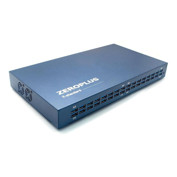
| ZeroPlus LAP-F 40/64-Channel | Watch | 40 or 64 channels with Quad SPI, SPI Plus and Samsung K9 NAND protocol analysis | £1,350 |
| Acute TravelLogic 34-Channel | Watch | Logic analyser running Acute's decoder library: Serial Flash/SPI Flash, QSPI from single to octal I/O, and SPI-NAND; parallel NAND decoders are supplied on request from Acute | £1,161.65 |
| Acute LA4000 Series | Watch | 68 or 136 channels at higher sample rates; runs Acute's SDR SDRAM decoder, with HyperBus and Serial PSRAM decoders available on request from Acute; these need the LA4000, LA3000+ or BusFinder series | £7,100 |
| Acute BusFinder BF6264 Pro | Watch | Acute's high-end bus analyser for wide, fast memory buses; same decoder library, with HyperBus available on request from Acute | £11,500 |
Programmers and Host Adapters
| Product | Role | Capability | Price ex VAT |
|---|---|---|---|
| Dediprog SF100 | Drive | In-system programmer for SPI NOR flash on the board, through an ISP header or test clip | £290 |
| Promira with SPI Active Level 3 (TP600710) | Drive | Single, Dual and Quad SPI controller to 80 MHz for scripted flash reads, writes and tests | £810 plus the £1,040 Promira |
| TP280210 High-Speed SPI Flash Demo Board | A known-good SPI NOR flash target (Winbond W25Q32JV, board rated to 50 MHz) for proving a set-up | £89 |
For SPI basics, clock modes and single-line analysers, see our SPI guide; for managed NAND, see SD, SDIO and eMMC. Tell us the flash part and bus speed and we will recommend a set-up.
Frequently Asked Questions
What Is SFDP?
Serial Flash Discoverable Parameters, JEDEC JESD216. A table inside the flash, read with command 5Ah, that lists its size, supported read commands, dummy cycles and erase sizes. Boot ROMs and drivers use it to work with flash from different vendors without a hard-coded part list.
What Is the Difference Between SPI NOR and SPI NAND?
SPI NOR is read directly at any address, suits code storage and execute-in-place, and has smaller capacities. SPI NAND is read and written a page at a time through an internal buffer, needs bad block management, and is cheaper per bit for larger capacities.
Can a Logic Analyser Capture Octal DDR Flash?
Only with enough sample rate and channels: at 200 MHz DDR you need well over 1 GS/s in timing mode, or a state mode that samples on both clock edges. Many engineers capture at a reduced clock rate during bring-up, which is usually where boot problems show.
Is HyperBus the Same as Octal SPI?
No, although both use eight DDR data lines. HyperBus has a fixed 48-bit command-address and a read-write data strobe signal; Octal SPI uses SPI-style commands, addresses and dummy cycles. Some controllers support both.
Where to Start with Flash Memory Buses
 ZeroPlus LAP-F High-Performance PC-Based Logic Analyser 40/64 Channel
£1,350.00
ex VAT Acute Technology TravelLogic 34-Channel Logic Analyser
From £1,161.65
ex VAT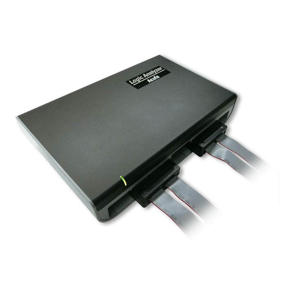 Acute Technology LA4000 Series 68/136 Ch Logic Analyser
From £7,100.00
ex VAT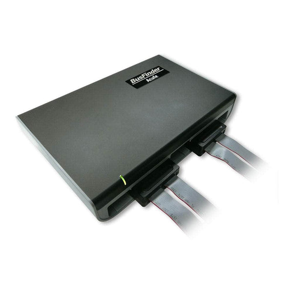 Acute BusFinder BF7264 Pro Protocol Analyser
£11,500.00
ex VAT
More Protocols
By John Legg CEng, Director, Debug Store. Updated 12 November 2026.
