
SWD (Arm Serial Wire Debug)
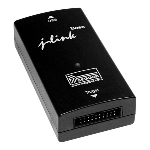
SWD (Serial Wire Debug) is Arm's two-wire debug interface: a clock (SWCLK) and one bidirectional data line (SWDIO) give a debugger the same access to a Cortex core's memory and debug registers as four-wire JTAG, on far fewer pins. To debug and program over SWD, use a probe such as the SEGGER J-Link BASE, which supports both SWD and JTAG. To see the packets themselves, a logic analyser with an SWD decoder shows each request, acknowledge and data word.
How SWD Is Wired
The probe drives SWCLK. SWDIO carries data both ways, so the probe and the target take turns driving it, with a turnaround cycle between them. Most Cortex-M parts that offer both interfaces put SWDIO on the JTAG TMS pin and SWCLK on TCK, which is why the same 10-pin and 20-pin debug headers work for both. A probe switches such a port from JTAG to SWD by sending a defined bit sequence after reset.
SWO (Serial Wire Output) is a separate, optional pin the target uses to stream trace data such as printf output, interrupt events and data watchpoints without stopping the core. It shares the JTAG TDO pin on many devices, so it is only available while the port is in SWD mode.
How an SWD Transaction Works
- Line reset: at least 50 SWCLK cycles with SWDIO high put the debug port in a known state. The probe then reads the debug port identification register (DPIDR) to confirm the connection.
- Request: 8 bits from the probe say whether this is a debug port or access port register, read or write, which register address, and a parity bit.
- Acknowledge: after a turnaround cycle, the target replies OK, WAIT (busy, try again) or FAULT (a sticky error flag is set). No reply at all usually means a wiring or power problem.
- Data: 32 bits and a parity bit, from the probe for a write or from the target for a read.
Everything a debugger does, from halting the core to programming flash, is built from these 32-bit register reads and writes through the debug and access ports.
SWD Compared with JTAG
| SWD | JTAG | |
|---|---|---|
| Signal pins | 2 (SWCLK, SWDIO) | 4 or 5 (TCK, TMS, TDI, TDO, TRST) |
| Cores | Arm only | Any device with a JTAG TAP |
| Several devices | Multi-drop, from SWD protocol version 2 (ADIv5.1) | Daisy chain |
| Boundary scan | No | Yes, on IEEE 1149.1 devices |
| Trace output | SWO on a spare pin | TDO is in use, so no SWO |
Where SWD Is Used
- Cortex-M microcontrollers: the default debug and programming port on most STM32, nRF, LPC, Kinetis, SAM, RP2040 and similar parts.
- Production programming: two signal pins fit on small boards and pogo-pin test pads, often through a Tag-Connect footprint.
- Field debugging: SWO trace gives live logging from a running product without a UART.
- Multi-core SoCs: Cortex-A and Cortex-R debug through the same Arm debug port model, often alongside JTAG.
Common SWD Faults and How to Find Them
| Symptom | Likely Cause | What to Check |
|---|---|---|
| "No target found" or no ACK | No target power, VTref not connected, or SWDIO and SWCLK swapped | Check VTref first, then capture SWDIO during the connect attempt |
| Repeated WAIT responses | The core or bus is busy, for example a flash operation or a clock not running | Lower the SWD clock and check the target clock configuration |
| FAULT after a memory access | An access to an invalid address or a protected region set a sticky error | Read the debug port status register and clear the sticky flags |
| Connects, then drops after code runs | Firmware reuses the SWD pins as GPIO, disables debug or enters deep sleep | Connect under reset, or hold the device in reset while attaching |
| Device locked, cannot connect at all | Read-out protection or a debug lock is enabled | Use the vendor's unlock or mass-erase procedure, which erases the flash. Some locks, such as STM32 RDP Level 2, are permanent and cannot be removed |
Tools for SWD Debugging and Analysis
Drive tools are debug probes that control the target over SWD. Watch tools capture SWCLK and SWDIO so you can see exactly what a probe sent and how the target answered.
Debug Probes
| Product | Role | Capability | Price ex VAT |
|---|---|---|---|
| SEGGER J-Link BASE Classic | Drive | SWD and JTAG debug probe with SWO, download to RAM up to 1 MB/s at up to 15 MHz, 1.2 V to 5 V targets | £470 |
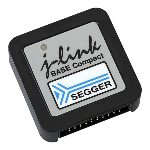
| SEGGER J-Link BASE Compact | Drive | The BASE in a smaller housing with a USB-C host connector | £470 |
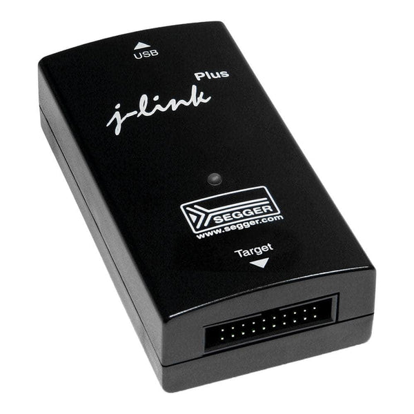
| SEGGER J-Link PLUS Classic | Drive | As BASE, with additional SEGGER software licences included | £660 |
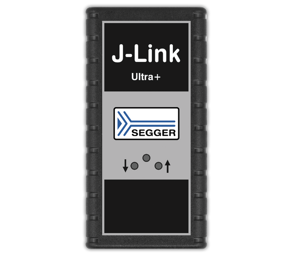
| SEGGER J-Link ULTRA+ | Drive | Faster model, download to RAM up to 4 MB/s at up to 50 MHz | £870 |
| SEGGER J-Link PRO | Drive | Up to 4 MB/s at up to 50 MHz, with 100 Mbit Ethernet as well as USB | £1,100 |
Logic Analysers with SWD Decoding
| Product | Role | Capability | Price ex VAT |
|---|---|---|---|
| Saleae Logic 8 | Watch | SWD decoder in the Logic 2 software shows requests, ACKs and data words | £405 |
| Saleae Logic Pro 8 | Watch | Higher sample rates for faster SWD clocks; same decoder | £830 |
Connecting Without a Header
- SEGGER J-Link 6-Pin Needle Adapter (£110) and 10-Pin Needle Adapter (£114): spring-pin adapters that press onto pads on the PCB, so no connector needs fitting. The 6-pin carries SWD only; the 10-pin carries SWD and JTAG.
- Tag-Connect TC2050-ARM2010 Adapter (£44): connects an Arm 20-pin probe such as J-Link to a TC2050-IDC Plug-of-Nails cable, so the board needs only a footprint, not a header.
Browse our debuggers collection, or tell us the target and we will recommend a probe and connection method.
Frequently Asked Questions
Can I Use SWD on a Non-Arm Chip?
No. SWD is part of the Arm Debug Interface and only Arm-based devices implement it. RISC-V and other cores use JTAG or their own two-wire schemes.
Do I Need SWO?
Not for debugging or programming. SWO adds non-intrusive trace output such as printf logging and event timing, which is worth routing to the debug header if the pin is free.
What Is the Minimum SWD Header?
SWDIO, SWCLK, ground and VTref. Adding nRESET lets the probe connect under reset, which recovers devices whose firmware disables the debug pins.
Is SWD Faster Than JTAG?
Often slightly, yes. Arm's figures show SWD moving more data per clock than JTAG memory access, and in practice the probe and target flash speed usually set the limit. SWD's main advantage is pin count.
Where to Start with SWD
More Protocols
By John Legg CEng, Director, Debug Store. Updated 3 November 2026.
