
JTAG (IEEE 1149.1)
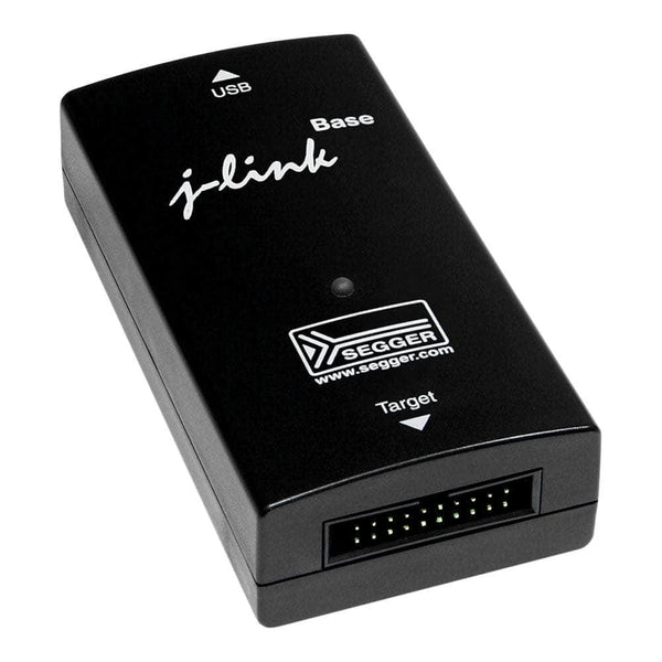
JTAG (IEEE 1149.1) is a four or five-wire test access port built into most microprocessors, FPGAs and CPLDs and many microcontrollers: TCK, TMS, TDI and TDO, plus optional TRST. It was designed for boundary-scan testing of solder joints and is now the standard route for debugging, programming flash and configuring FPGAs. To debug and program Arm, RISC-V and many other cores, use a debug probe such as the SEGGER J-Link BASE. To see the TAP signals themselves, a logic analyser with a JTAG decoder shows each state change and shifted value.
How JTAG Is Wired
The probe drives TCK and TMS to every device in parallel. TDI and TDO form a ring: data enters the first device, comes out of its TDO into the next device, and the last TDO returns to the probe. Each device in the chain adds its instruction register to an IR scan and its selected data register to a DR scan, so the probe software must know the chain order and register lengths, usually from each device's BSDL file or by reading the IDCODEs after reset.
Most debug connectors also carry a target reference voltage (VTref) so the probe matches the target's logic level, and a system reset line (nRESET or nSRST) separate from TRST. Common headers are the 20-pin 0.1 inch Arm connector and the 10-pin and 20-pin 0.05 inch Cortex debug connectors, which carry SWD on the same pins.
How the TAP Controller Works
- Reset: five or more TCK cycles with TMS high put every TAP into Test-Logic-Reset, whatever state it was in. Asserting TRST, where fitted, does the same.
- Select a register: an instruction register (IR) scan loads an instruction such as IDCODE, BYPASS, EXTEST or a vendor debug command. That instruction decides which data register sits between TDI and TDO.
- Capture: the chosen data register loads its current value in parallel, for example the pin states in a boundary-scan register.
- Shift: with TMS low, each TCK shifts one bit in on TDI and one bit out on TDO. The bits coming out are what was captured.
- Update: the shifted-in value is latched into the register's outputs, for example driving pins or writing a debug register.
Devices not being addressed are put in BYPASS, which makes each of them a single-bit delay in the chain.
What JTAG Is Used For
| Use | What Happens | Typical Tool |
|---|---|---|
| Debugging | Halt, step, set breakpoints and read memory through the core's debug logic | Debug probe with an IDE or GDB server |
| Flash programming | Load code into on-chip or external flash through the debug interface | Debug probe or production programmer |
| FPGA and CPLD configuration | Load a bitstream or program configuration memory | Vendor cable or compatible probe |
| Boundary-scan test | Drive and read pins to find opens and shorts on assembled boards without bed-of-nails access | Boundary-scan software with a JTAG controller |
Variants
IEEE 1149.7, often called cJTAG, carries JTAG over two pins (TCKC and TMSC) and adds a star topology. Arm cores also offer SWD, a two-wire debug protocol that replaces JTAG for debugging but not for boundary scan. See the SWD page for how it compares.
Common JTAG Faults and How to Find Them
| Symptom | Likely Cause | What to Check |
|---|---|---|
| Probe reports no device or IDCODE of all 0s or all 1s | TDO not reaching the probe, no target power, or VTref not connected | Check VTref, then capture TDO during an IDCODE scan |
| Chain length or IDCODEs wrong | A device missing from or added to the chain, or a broken TDO to TDI link | Compare the read IDCODEs with the expected chain order |
| Works at low speed, fails at full speed | Long cable, reflections on TCK, or a slow device in the chain | Lower the JTAG clock; use adaptive clocking (RTCK) where the core supports it |
| Connects once, then fails after reset | Firmware reconfigures the JTAG pins as GPIO or enters a low-power mode | Connect under reset, or hold the device in reset while attaching |
| Intermittent errors on a noisy or high-voltage system | Ground loops or common-mode noise between PC and target | Use a galvanic isolator between probe and target |
Tools for JTAG Debugging and Analysis
Drive tools control the TAP to debug, program or test the target. Watch tools capture TCK, TMS, TDI and TDO so you can see exactly what a probe or a boundary-scan program sent.
Debug Probes
| Product | Role | Capability | Price ex VAT |
|---|---|---|---|
| SEGGER J-Link BASE Classic | Drive | JTAG and SWD debug probe, JTAG to 15 MHz, download to RAM up to 1 MByte/s, 1.2 V to 5 V targets | £470 |
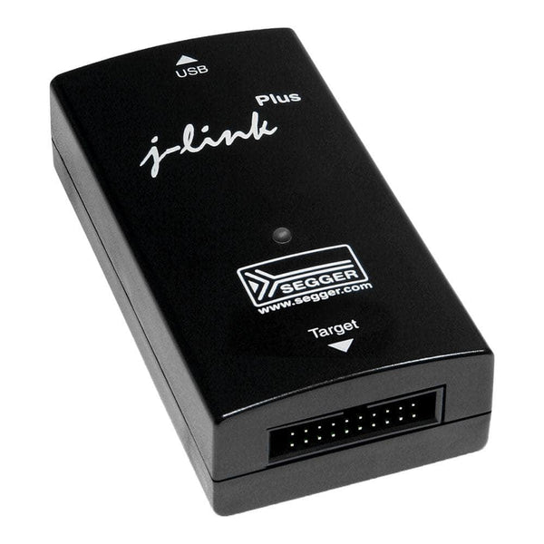
| SEGGER J-Link PLUS Classic | Drive | As BASE, with licences for J-Flash, Unlimited Flash Breakpoints, Ozone, Monitor Mode Debugging and RDI included | £660 |
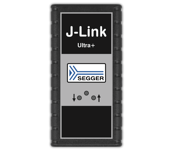
| SEGGER J-Link ULTRA+ | Drive | JTAG to 50 MHz, download to RAM up to 4 MBytes/s | £870 |
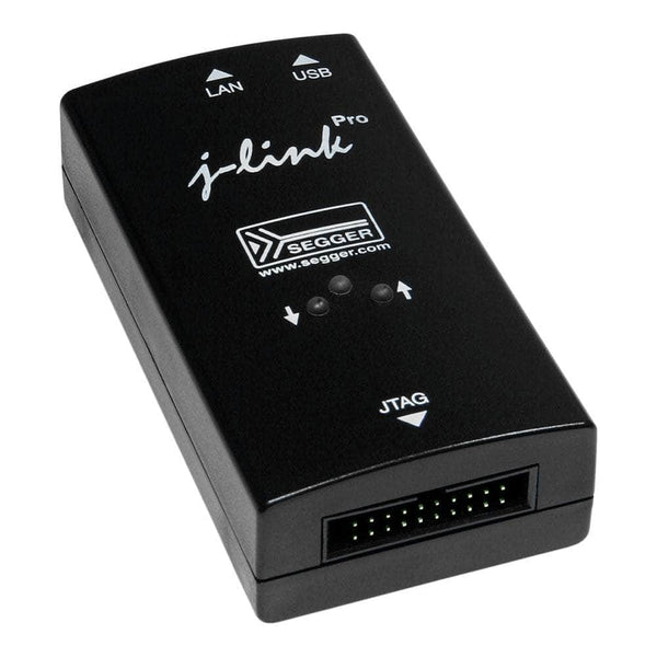
| SEGGER J-Link PRO | Drive | JTAG to 50 MHz, up to 4 MBytes/s, with Ethernet as well as USB | £1,100 |
Logic Analysers with JTAG Decoding
| Product | Role | Capability | Price ex VAT |
|---|---|---|---|
| Saleae Logic 8 | Watch | JTAG decoder in the Logic 2 software shows each TAP state with the TDI and TDO data shifted in it | £405 |
| Saleae Logic Pro 16 | Watch | 16 channels for JTAG plus reset, trace or other buses | £1,245 |
Isolation and Connection
- SEGGER J-Link JTAG Isolator (£226): 1 kV DC basic isolation between probe and target, JTAG to 4 MHz, 1.2 V to 5 V. It does not pass SWD or cJTAG.
- Tag-Connect TC2050-ARM2010 Adapter (£44): connects an Arm 20-pin probe such as J-Link to a TC2050 plug-of-nails cable, so the board needs only a footprint, not a header.
- Tag-Connect TC2050-2x10 Adapter (£40): splits a 0.1 inch 20-pin JTAG header into two 10-pin headers, each for a TC2050-IDC cable, for tools such as XJTAG.
Browse our debuggers and logic analysers collections, or tell us the target core and we will recommend a probe.
Frequently Asked Questions
What Is the Difference Between JTAG and SWD?
JTAG uses four or five wires, can chain many devices, and supports boundary scan. SWD is Arm's two-wire debug protocol: it does the same debugging job with fewer pins but works on Arm cores only, does not daisy-chain in the same way, and has no boundary scan.
Does Every Chip with JTAG Support Boundary Scan?
Not always. Boundary scan needs the device to implement the IEEE 1149.1 boundary-scan register and publish a BSDL file. Many microcontrollers use the JTAG port only for debug.
How Fast Can JTAG Run?
The probe and the slowest device in the chain set the limit. Many cores limit TCK relative to their own clock, which is why adaptive clocking with RTCK exists. The J-Link BASE and PLUS run JTAG to 15 MHz and the ULTRA+ and PRO to 50 MHz.
What Is TRST For?
TRST is an optional asynchronous reset for the test logic only. Without it, five TCK cycles with TMS high do the same job. It is separate from the system reset that restarts the processor.
Why Can I Not Connect After My Firmware Starts?
The firmware may switch the JTAG pins to other functions, disable debug, or put the core to sleep. Connecting while the device is held in reset usually gets the probe in before that code runs.
Where to Start with JTAG
By John Legg CEng, Director, Debug Store. Updated 3 November 2026.
