Overview
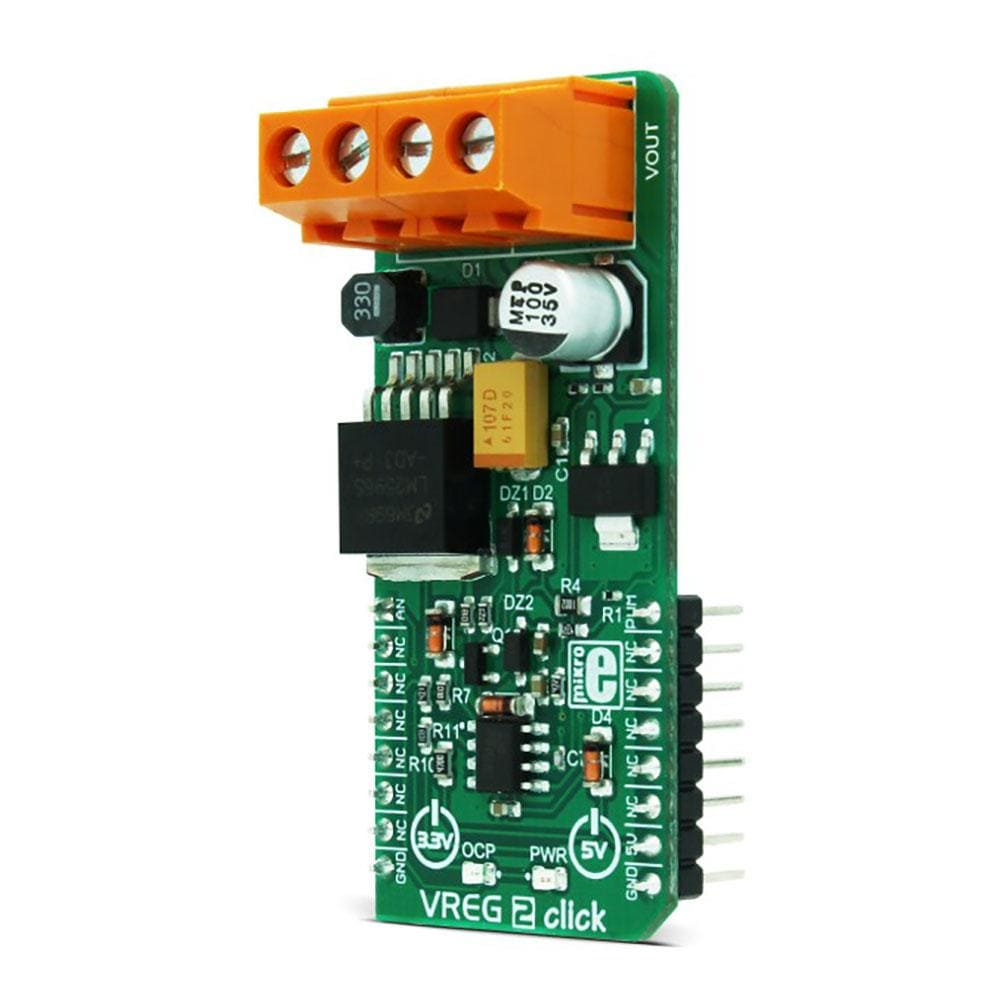
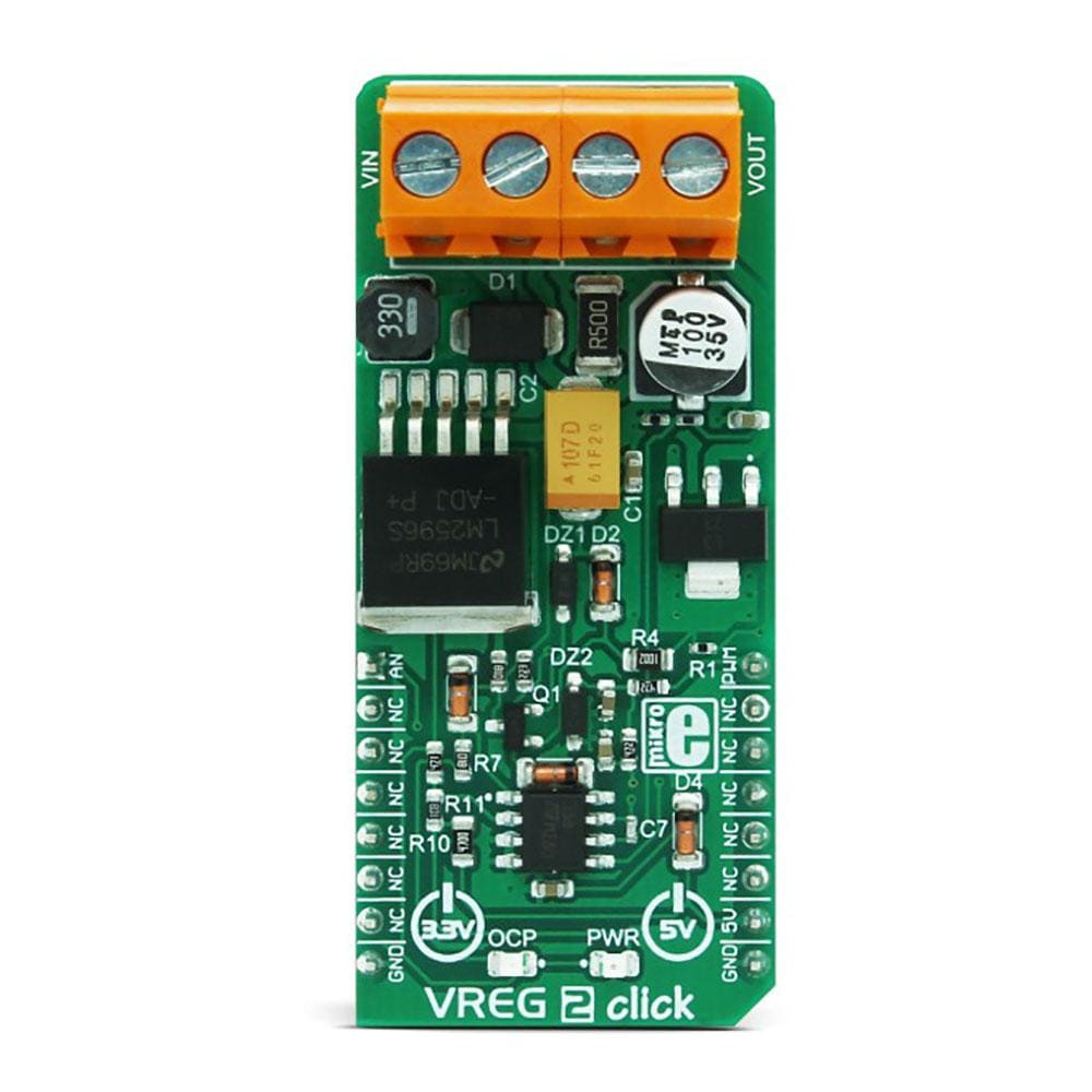
The VREG 2 Click Board™ is a voltage regulator Click Board™, with outstanding performance. It has a steady output voltage with the ripple lower than 5mV, short circuit protection with the LED indicator, and high efficiency with minimal power dissipation. The main output regulation element is the LM317, a well-established adjustable voltage regulator, often used in various electrical designs, for its outstanding regulation characteristics. The supporting electronics allows for reduced dissipation, voltage regulation and short-circuit indication. It consists of the LM358, a dual operational amplifier (op-amp) with high voltage gain, and the LM2596 buck converter.
The VREG 2 Click Board™ can be used with the input voltage in the range of 10V to 35V, and output voltage in the range of 2.5V to 15V, with current up to 600mA.
Downloads
The VREG 2 Click Board™ is a voltage regulator click, with outstanding performances. It has a steady output voltage with the ripple lower than 5mV, short circuit protection with the LED indicator, and high efficiency with minimal power dissipation. The main output regulation element is the LM317, a well-established adjustable voltage regulator, often used in various electrical designs, for its outstanding regulation characteristics. The supporting electronics allows for the reduced dissipation, voltage regulation and short-circuit indication. It consists of the LM358, a dual operational amplifier (op-amp) with high voltage gain, and the LM2596 buck converter. The VREG 2 Click Board™ can be used with the input voltage in the range of 10V to 35V, and output voltage in the range of 2.5V to 15V, with current up to 600mA.
Due to its performance, the VREG 2 Click Board™ can be used for applications which require low ripple regulated voltage within a range between 2.5V and 15V. It can be also used for wall adapter regulators, general purpose power supplies, distributed supply regulators, and similar applications where voltage regulation with the low ripple and wide input voltage range is required.
How Does The VREG 2 Click Board™ Work?
The electrical circuit on the VREG 2 Click Board™ consists of two voltage regulators of which one is a linear voltage regulator, while the second is a switching step down converter also known as the buck converter. Such topology combines the benefits of both worlds: linear regulator offers very low voltage ripple and noise, while the switching regulator provides optimal working conditions, avoiding large voltage difference between the input and output voltage of the linear regulator. Unlike the buck converter, a large difference between the input and the output voltage on the linear regulator lead to significant dissipation losses.
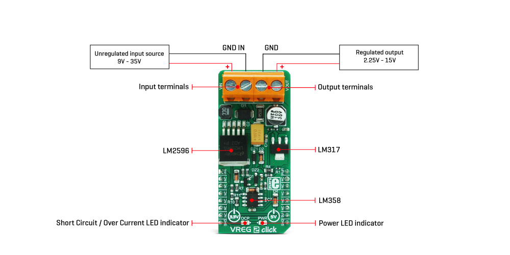
The VREG 2 Click Board™ uses the LM2596, a 3A, step down voltage regulator working at 150 kHz, from Texas Instruments. It belongs to Simple Switcher™ line of products, meaning that it supports both continuous and discontinuous modes. This buck DC-DC converter itself can handle from 4.5V up to 40V, but the circuit works reliably with voltages in the range between 9V and 35V. This IC has a reasonably simple layout with just a few external pins. The output voltage of the DC-DC converter is regulated by the feedback loop. Normally, there is a voltage divider with its center pin routed to the FB pin of the LM2596, but on this Click board™, there is a PNP BJT with the 2.7V Zener diode on its emitter, which is used to provide about 3V more voltage on its output, than the desired target voltage. This provides an ideal voltage headroom for the linear regulator, allowing for greater efficiency and less power dissipation.
The linear voltage regulator is LM317, a well-established three terminal adjustable voltage regulator, from Texas Instruments. This IC is used on many voltage regulation designs, as it is very simple, reliable and does not require a big number of external components. The input voltage is provided from the LM2596 and as already mentioned, this voltage is about 3V greater than the target regulation voltage, allowing optimal headroom for LM317 IC. The ADJ pin is used to set the output voltage on this IC. It is driven by the output of the first op-amp of the LM358 IC, a dual operational amplifier, from Texas Instruments. The non-inverting input of this op-amp is controlled by the PWM signal from the MCU and therefore, the mikroBUS™ PWM pin is routed to this non-inverting input. By applying an additional RC filter, PWM signal is converted to a constant linear voltage ranging up to 3.3V, as it is limited by another Zener diode on this input. The inverting pin of this op-amp is connected to an output voltage divider, with its center tap at 3.3V for the maximum output voltage of 15V. This allows the output voltage to be measured by the host MCU. Therefore, this pin is routed to the mikroBUS™ AN pin.
The short circuit protection section is designed with the second op-amp of the LM358 IC, working as a comparator. When the current starts flowing through the 0.5Ω resistor, in the event of a short circuit on the output, it will cause rising of the op-amp output voltage. The red LED indicator labeled as OCP will be lit, indicating the short circuit condition. This will also cause the rising of the FB voltage of the buck regulator, effectively blocking its operation and cutting the power to the output.
NOTE: Do not connect GND IN to the GND externally, these rails should remain separated and connected to the respective terminal inputs on the Click board™ itself.
SPECIFICATIONS
| Type | Buck |
| Applications | The VREG 2 Click Board™ can be used for precise voltage regulators, wall adapter regulators, general purpose power supplies, distributed supply regulators, and similar applications where voltage regulation with the low ripple and wide input voltage range is required. |
| On-board modules | LM2596, a 3A, step down voltage regulator working at 150 kHz, from Texas Instruments; LM317, a three terminal adjustable voltage regulator, from Texas Instruments; LM358, a dual operational amplifier from Texas Instruments. |
| Key Features | Low output voltage ripple, high efficiency and low dissipation losses, overcurrent and short circuit protection, thermal shutdown, a wide range of input voltage, adjustable voltage via PWM, output voltage read-out by the host MCU. |
| Interface | Analog,PWM |
| Compatibility | mikroBUS |
| Click board size | L (57.15 x 25.4 mm) |
| Input Voltage | 3.3V,5V |
PINOUT DIAGRAM
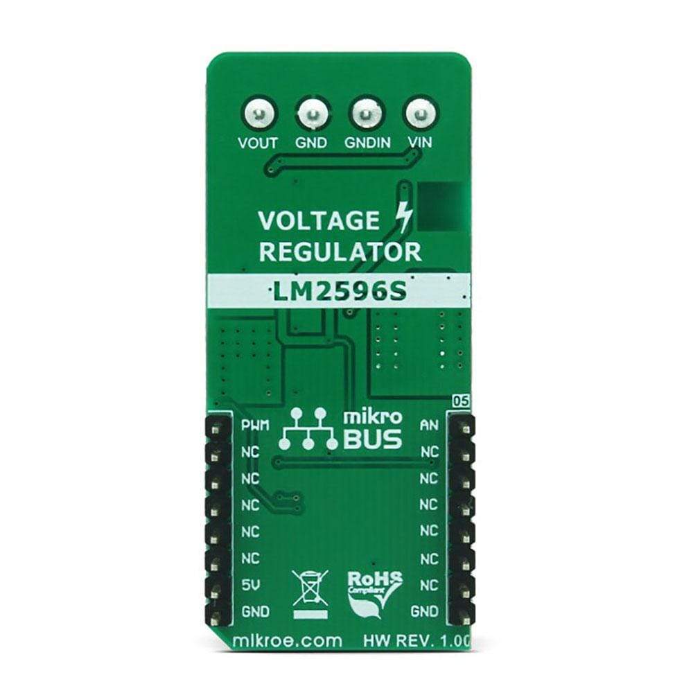
This table shows how the pinout of the VREG 2 Click Board™ corresponds to the pinout on the mikroBUS™ socket (the latter shown in the two middle columns).
| Notes | Pin |  |
Pin | Notes | |||
|---|---|---|---|---|---|---|---|
| Voltage sensing | AN | 1 | AN | PWM | 16 | PWM | Control PWM |
| NC | 2 | RST | INT | 15 | NC | ||
| NC | 3 | CS | RX | 14 | NC | ||
| NC | 4 | SCK | TX | 13 | NC | ||
| NC | 5 | MISO | SCL | 12 | NC | ||
| NC | 6 | MOSI | SDA | 11 | NC | ||
| NC | 7 | 3.3V | 5V | 10 | +5V | Power Supply | |
| Ground | GND | 8 | GND | GND | 9 | GND | Ground |
VREG 2 CLICK ELECTRICAL SPECIFICATIONS
| Description | Min | Typ | Max | Unit |
|---|---|---|---|---|
| Input voltage | 9 | - | 35 | V |
| Output voltage | 2.25 | - | 15 | V |
| Output current | - | 0.5 | 0.6 | A |
| Short Circuit Current | 0.8 | 0.9 | 1.5 | A |
ONBOARD SETTINGS AND INDICATORS
| Label | Name | Default | Description |
|---|---|---|---|
| LD1 | PWR | - | Power LED indicator |
| LD2 | OCP | - | Short circuit/overcurrent protection LED indicator |
| TB1 | VIN | - | Input power supply connection terminal |
| TB2 | VOUT | - | Regulated output connection terminal |
| General Information | |
|---|---|
Part Number (SKU) |
MIKROE-3055
|
Manufacturer |
|
| Physical and Mechanical | |
Weight |
0.027 kg
|
| Other | |
Country of Origin |
|
HS Code Customs Tariff code
|
|
EAN |
8606018713134
|
Warranty |
|
Frequently Asked Questions
Have a Question?
Be the first to ask a question about this.


