


Picotest
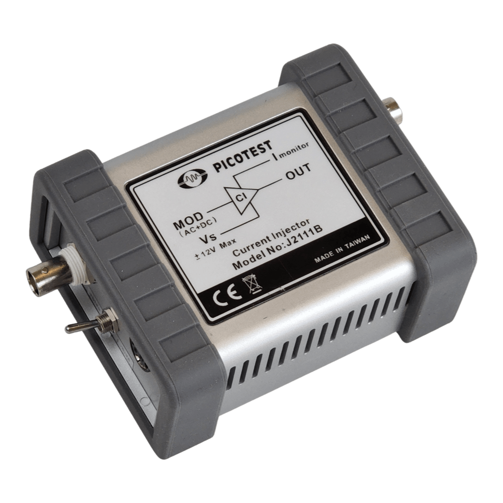
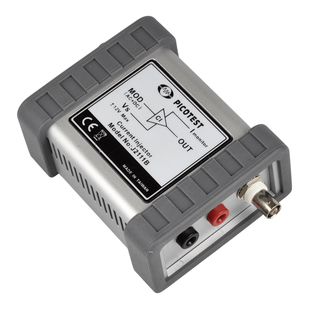
Picotest J2111B Current Injector
Picotest J2111B Current Injector
SKU: J2111B
Couldn't load pickup availability
Key Features
Overview
The Picotest J2111B Current Injector stands as the most versatile tool in the signal injector family, combining bidirectional operation with 40 MHz bandwidth for comprehensive power supply characterisation. Designed for engineers who demand precision, it transforms vector network analysers and oscilloscopes into complete power integrity test systems. The J2111B sinks current from positive or negative voltage sources, making it suitable for everything from 1.8 V mobile processors to 48 V automotive systems.
Pair the J2111B with the Picotest G5100A Arbitrary Waveform Generator to generate load step waveforms with controlled rise/fall times, simulating real-world digital circuit loading. Alternatively, connect to a Bode 100 Vector Network Analyser for swept impedance measurements and Non-Invasive Stability Measurement (NISM) analysis. The built-in bias current enables Class A operation with network analysers, eliminating the need for external DC sources.
Three-port impedance measurements become straightforward: inject current through the J2111B, monitor current via the 50 Ω output, and measure voltage with a probe. The analyser calculates impedance as voltage divided by current (V/I), revealing resonances, control loop bandwidth, and damping characteristics that determine system stability and transient response.
Downloads
Why Engineers Choose The Picotest J2111B Current Injector
Bidirectional Capability
True Non-Invasive Testing
NISM Phase Margin Analysis
High-Bandwidth Current Injection for Power Integrity Analysis
The Picotest J2111B Current Injector delivers uncompromising performance for power supply output impedance measurement, non-invasive stability testing, and high-speed load transient analysis. Engineered for demanding applications where precision matters, this voltage-controlled current sink operates from DC to 40 MHz with typical rise and fall times of 20 nanoseconds, enabling accurate characterisation of modern switching regulators, LDOs, and PDN architectures.
Bidirectional Operation for Maximum Versatility
Unlike unipolar alternatives, the J2111B features two-quadrant operation, sinking current from either positive or negative voltage sources. This bipolar capability supports testing across voltage ranges from +1.5 V to +60 V and -1.5 V to -60 V, accommodating everything from low-voltage point-of-load regulators to automotive and industrial power systems. The controllable output current variation spans 50 mA, with an additional ±25 mA DC offset providing a total range of 74 mA peak.
Built-In Current Monitoring and 50 Ω Integration
A precision current monitor output delivers 1 V per amp scaling into 50 Ω, integrating seamlessly with vector network analysers, oscilloscopes, and DMMs. The modulation input accepts signals from arbitrary waveform generators (such as the Picotest G5100A), function generators, or network analysers. With 10 mA/V voltage-to-current scaling (40 dB attenuation), the J2111B enables precise control of injected current profiles for load step testing, PDN impedance sweeps, and control loop stability analysis.
Three-Port Impedance Measurement
When paired with a voltage probe and network analyser, the J2111B facilitates three-port impedance measurements, calculating output impedance as the voltage-to-current ratio (V/I). This technique proves invaluable for measuring regulator output impedance, battery impedance, and power bus characterisation. The method works particularly well for voltages ≥12 V where the 25 mA bias current represents a minor perturbation.
| Parameter | Specification | Unit |
|---|---|---|
| Output Current Variation (Controllable) | 50 | mA |
| Total Output Current (Controllable + Bias) | 74 | mA |
| Modulator Gain | 10 | mA/V |
| Current Monitor Scaling | 1 | V/A |
| Usable Bandwidth | DC–40 | MHz |
| Rise/Fall Time (Typical) | 20 | ns |
| Absolute Output Voltage Range | -60 to -1.5, +1.5 to +60 | V |
| Max Input Voltage (DC+AC) | ±5 | V |
| Offset Current (Typical) | +24/0/-24 | mA |
| Modulation Input Impedance | 50 | Ω |
| Current Monitor Output Impedance | 50 | Ω |
| Operating Temperature | 0–50 | °C |
| Maximum Altitude | 6000 | ft |
| Absolute Maximum Voltage | <50 VAC, 75 VDC | — |
Non-Invasive Stability Measurement (NISM)
The J2111B enables Non-Invasive Stability Measurement, a technique that derives phase margin from output impedance data when traditional Bode plot access is unavailable. NISM proves particularly valuable for fixed-output LDOs, voltage references, and integrated POLs where feedback pins are inaccessible. When used with OMICRON Lab Bode 100 or Keysight E5061B analysers, NISM software converts impedance measurements into phase margin values accurate to within 1 degree of traditional control loop analysis.
High-Speed Load Transient Testing
Traditional electronic loads suffer bandwidth limitations, capacitive loading, and slow slew rates. The J2111B overcomes these constraints with minimal output capacitance and 20 nanosecond edges. Drive the injector with arbitrary waveforms to simulate battery discharge profiles, high-speed digital load currents, or spontaneous current spikes. The fast response reveals regulator behaviour under transient conditions that conventional e-loads cannot replicate, exposing stability margins, underdamped ringing, and voltage droop.
Power Supply and Included Accessories
The J2111B ships with the J2171A High PSRR Regulated Adapter, a purpose-designed universal input power supply (100–240 VAC). Unlike generic switching adapters that introduce ripple above 100 kHz, the J2171A employs discrete linear regulators with ultra-high power supply rejection ratio and exceptionally low output impedance at 40 MHz. This ensures the measurement noise floor remains uncompromised by supply-induced artefacts.
Comparison: J2111B vs J2112A
| Feature | J2111B | J2112A |
|---|---|---|
| Maximum Current Output | 75 mA (50 mA + 25 mA bias) | 1 A (240 mA minimum) |
| Voltage-to-Current Scaling | 10 mA/V | 200 mA/V |
| Polarity | Bidirectional (positive/negative) | Unipolar (positive only) |
| Voltage Range | -60 to -1.5 V, +1.5 to +60 V | +0.7 to +50 V |
| Bandwidth | DC–40 MHz | DC–50 MHz |
| Rise/Fall Time | 20 ns (typical) | 10 ns (typical) |
| Current Monitor Scaling | 1 V/A | 0.1 V/A |
| Best For | Low-current, bipolar supplies | High-current POL regulators |
Applications Beyond Power Supplies
The J2111B extends to transistor characterisation, extracting small-signal current gain, transition frequency (Ft), and dynamic parameters. In RF and instrumentation circuits, it provides constant-current biasing for Class A amplifiers and buffers. Battery impedance measurement benefits from the injector's ability to sink current without introducing significant capacitive loading, preserving the accuracy of electrochemical impedance spectroscopy.
Safety and Compliance
Absolute maximum ratings must be observed at all times to avoid equipment damage or injury. Ensure output voltage remains within -60 to -1.5 V or +1.5 to +60 V. Between -1.5 V and +1.5 V, the J2111B will not operate reliably. For full specification compliance, maintain output voltage above 1.5 V or below -1.5 V. Never exceed 50 VAC or 75 VDC on the output terminals.
Frequently Asked Questions
Have a Question?
-
How does the J2111B support transistor characterisation?
Connect the transistor collector/drain to the J2111B output, apply appropriate bias, and inject AC current whilst monitoring voltage. This reveals small-signal current gain (hfe or β), transition frequency (Ft), output impedance, and dynamic parameters. The 40 MHz bandwidth captures transistor behaviour well into the RF region, useful for amplifier design and modelling. The technique works for BJTs, JFETs, and MOSFETs in common-emitter/source configurations.
-
What voltage range limitations should I observe?
The J2111B operates from -60 to -1.5 V and +1.5 to +60 V. Between -1.5 V and +1.5 V, operation is unreliable as the internal circuitry requires sufficient compliance voltage. For full specification compliance, maintain output voltage above ±1.5 V. Never exceed 50 VAC or 75 VDC absolute maximum ratings to avoid equipment damage. Always verify the device under test voltage before connection.
-
Can the J2111B test switching regulators and DC-DC converters?
Absolutely. The J2111B measures switching regulator output impedance, revealing control loop bandwidth, output capacitor ESR/ESL, and stability margins. Load transient testing with arbitrary waveforms characterises voltage droop, recovery time, and undershoot/overshoot. Non-invasive stability measurement (NISM) derives phase margin from output impedance, checking stability without breaking feedback loops. The J2111B also measures input filter stability when combined with the negative resistance of the switching converter.
-
How do interconnection parasitics affect high-frequency measurements?
At 40 MHz, even short wire lengths introduce significant inductance that rolls off measurement bandwidth. Use short, low-inductance coax or wide PCB traces. Keep connections under 10 cm where possible. The quoted 20 ns rise/fall time and 40 MHz bandwidth are interconnection-dependent; excessive lead inductance degrades performance. For best results, position the J2111B close to the device under test.
-
What is the difference between the J2111B and J2112A current injectors?
The J2111B provides 75 mA maximum current (50 mA + 25 mA bias) with bidirectional operation for positive or negative supplies, whilst the J2112A delivers 1 A maximum (240 mA minimum) but only sources current for positive supplies. The J2111B offers wider voltage range (-60 to +60 V vs +0.7 to +50 V) but lower current capacity. Choose J2111B for low-current, bipolar applications; select J2112A for high-current POL regulators.
-
Why is the J2171A power adapter included rather than a standard supply?
Generic switching adapters introduce ripple above 100 kHz that passes through opamp power supply rejection, degrading the J2111B noise floor. The J2171A employs discrete linear regulators with ultra-high PSRR and exceptionally low output impedance at 40 MHz. This preserves measurement fidelity, particularly when characterising low-impedance PDNs or measuring sub-milliohm output impedance where supply noise becomes significant.
-
What equipment is needed for a complete three-port impedance measurement?
Three-port measurement requires a vector network analyser (such as the <a href="https://thedebugstore.com/products/omicron-lab-bode-100-vector-network-analyser-uk">Omicron Lab Bode 100</a> or Keysight E5061B), the J2111B current injector, a voltage probe, and optionally a ground loop breaker like the <a href="https://thedebugstore.com/products/picotest-j2102b-common-mode-transformer">Picotest J2102B</a>. The analyser stimulus drives the J2111B input, current is monitored via the J2111B output, and voltage is measured with a probe. Impedance equals voltage divided by current, calculated by the analyser.
-
How does Non-Invasive Stability Measurement (NISM) work?
NISM derives phase margin from output impedance measurements when traditional Bode plots are inaccessible. The J2111B injects current whilst monitoring output voltage. NISM software analyses the impedance magnitude and phase, identifying the characteristic impedance peak that correlates with control loop bandwidth. Phase margin is computed from peak height and sharpness, accurate to within 1 degree of conventional loop gain measurements. This proves invaluable for fixed-output LDOs, voltage references, and integrated POLs.
-
Can the J2111B measure battery impedance?
Yes. The J2111B excels at battery impedance measurement by sinking current without introducing significant capacitive loading. Connect the battery to the output terminals, inject a swept AC signal, and monitor voltage and current to calculate impedance. This technique reveals internal resistance, electrode polarisation, and electrochemical dynamics across the DC to 40 MHz range.
-
What distinguishes the J2111B from traditional electronic loads?
The J2111B offers 40 MHz bandwidth with 20 ns rise/fall times, vastly exceeding electronic load capabilities (typically <100 kHz). Its minimal output capacitance avoids loading the circuit under test, preserving measurement accuracy. The precision current monitor provides 1 V/A scaling directly compatible with vector network analysers, enabling swept impedance measurements impossible with conventional loads.