


Mikroelektronika d.o.o.
Boost 7 Click Board™
Boost 7 Click Board™
SKU: MIKROE-5575
Couldn't load pickup availability


Key Features
Overview
Boost Your Voltage with the Boost 7 Click Board™
Looking to step up the voltage for your load? Look no further than the Boost 7 Click Board™, the compact add-on board that delivers reliable voltage regulation for a range of applications.
Powerful Performance, Minimal Footprint
Featuring the advanced BD8316GWL dual DC/DC converter from Rohm Semiconductor, the Boost 7 Click Board™ is designed to provide up to 200mA current limit and generate well-regulated positive and negative outputs of ±3.3V or ±5V. This makes it ideal for a wide range of applications that require split rail operating voltages.
Versatile Compatibility
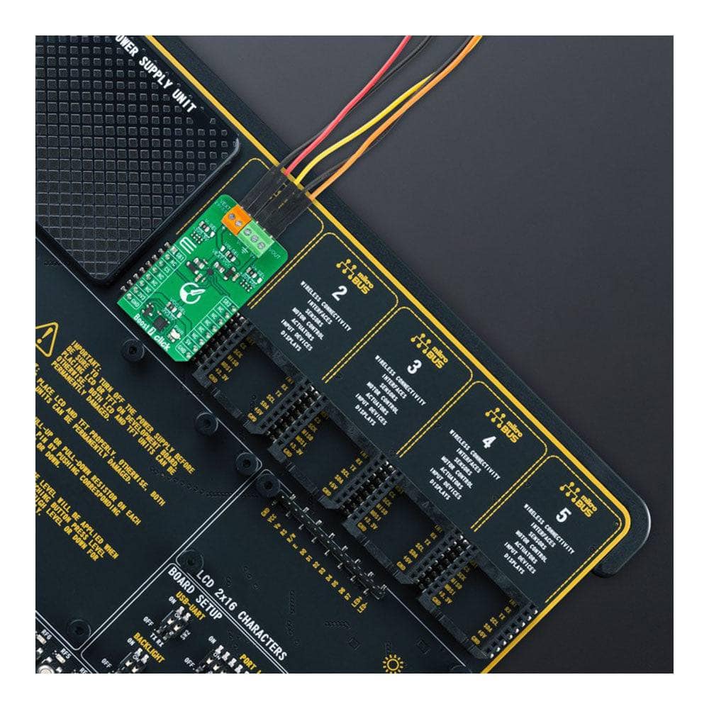
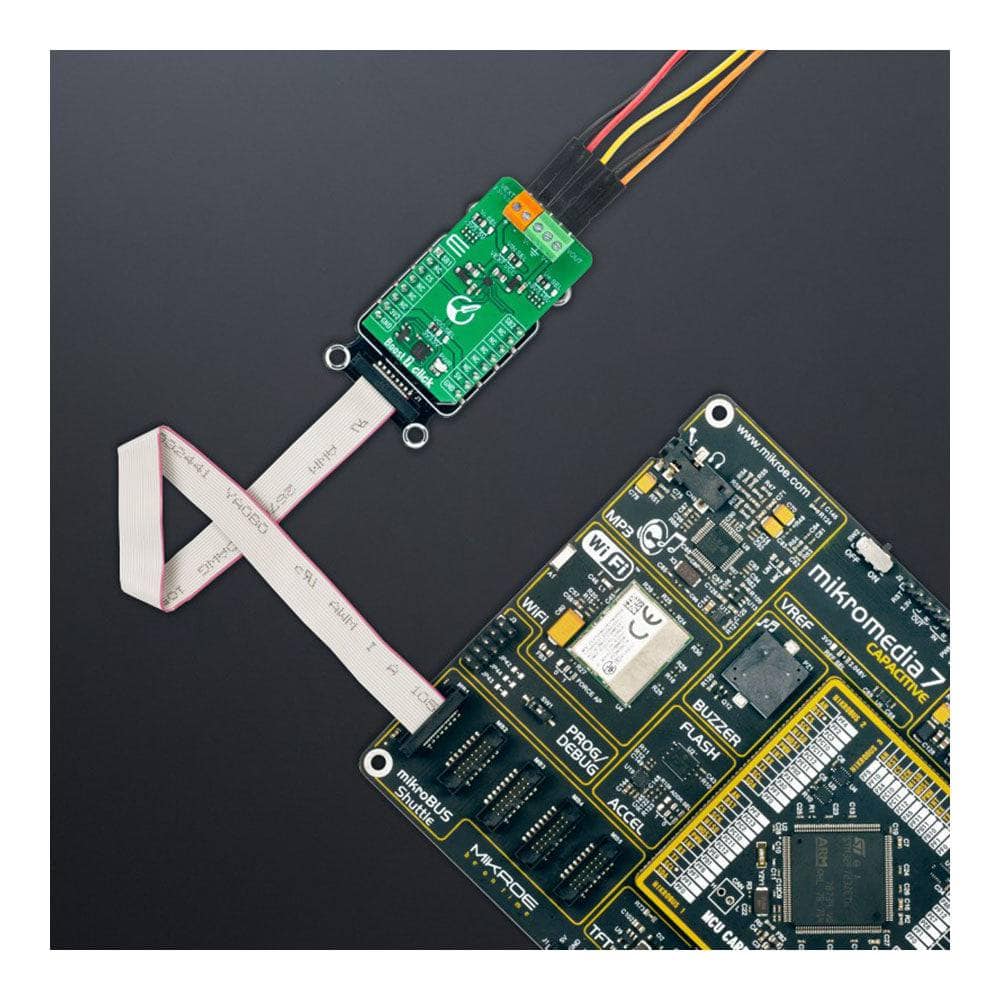
The Boost 7 Click Board™ is compatible with both mikroBUS™ power rails and also supports external power supply with a very low voltage of 2.5V. This gives you the flexibility you need to power your load no matter where you are.
Simplified Software Development
With the mikroSDK-compliant library, software development for the Boost 7 Click Board™ has never been easier. Our library includes functions that simplify software development, so you can get up and running quickly and easily.
Ready to Use
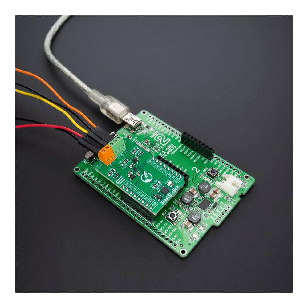
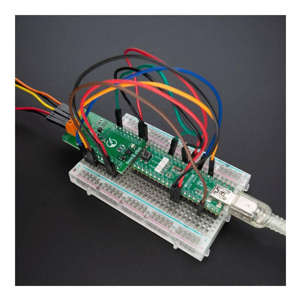
The Boost 7 Click Board™ comes fully tested and ready to use on any system equipped with the mikroBUS™ socket. So why wait? Boost your voltage and power up your applications with the Boost 7 Click Board™ today!Downloads
How Does The Boost 7 Click Board™ Work?
The Boost 7 Click Board™ is based on the LT1945, a dual step-up and inverted DC/DC converter from Rohm Semiconductor that boosts an input voltage to a higher level required by an output load. The BD8316GWL switching regulator feature integrated N-channel FETs and power P-channel MOSFETs alongside a Soft Start feature. Each converter inside the LT1945 is designed with up to 200mA current limit generating well-regulated positive and negative outputs of ±3.3V or ±5V, making the BD8316GWL ideal for various portable applications.
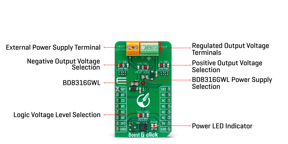
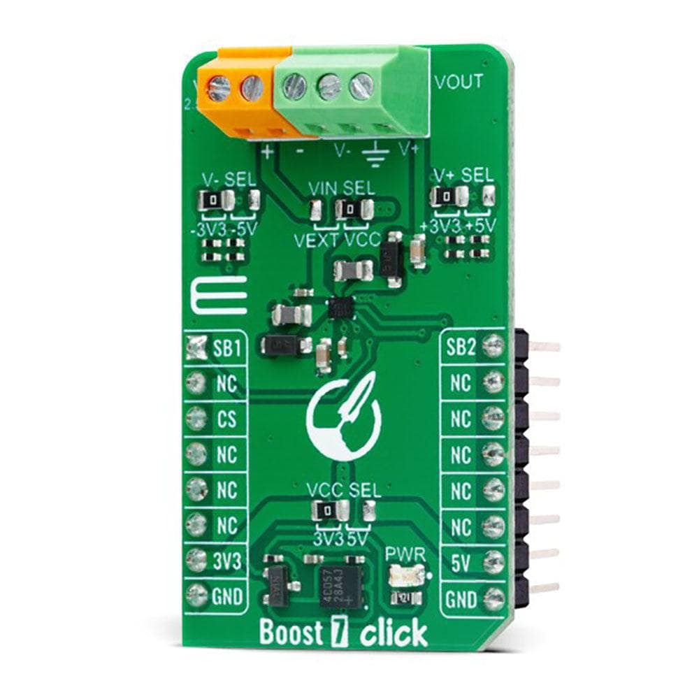
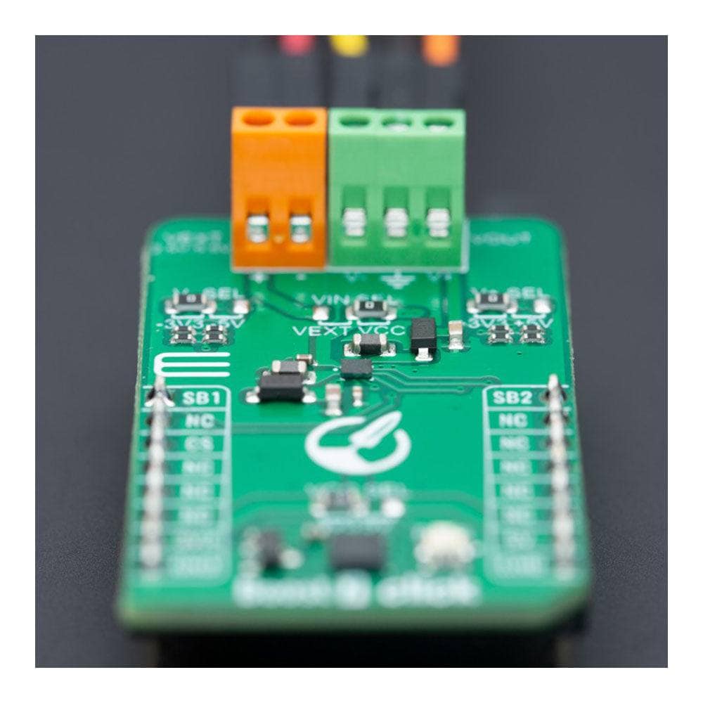
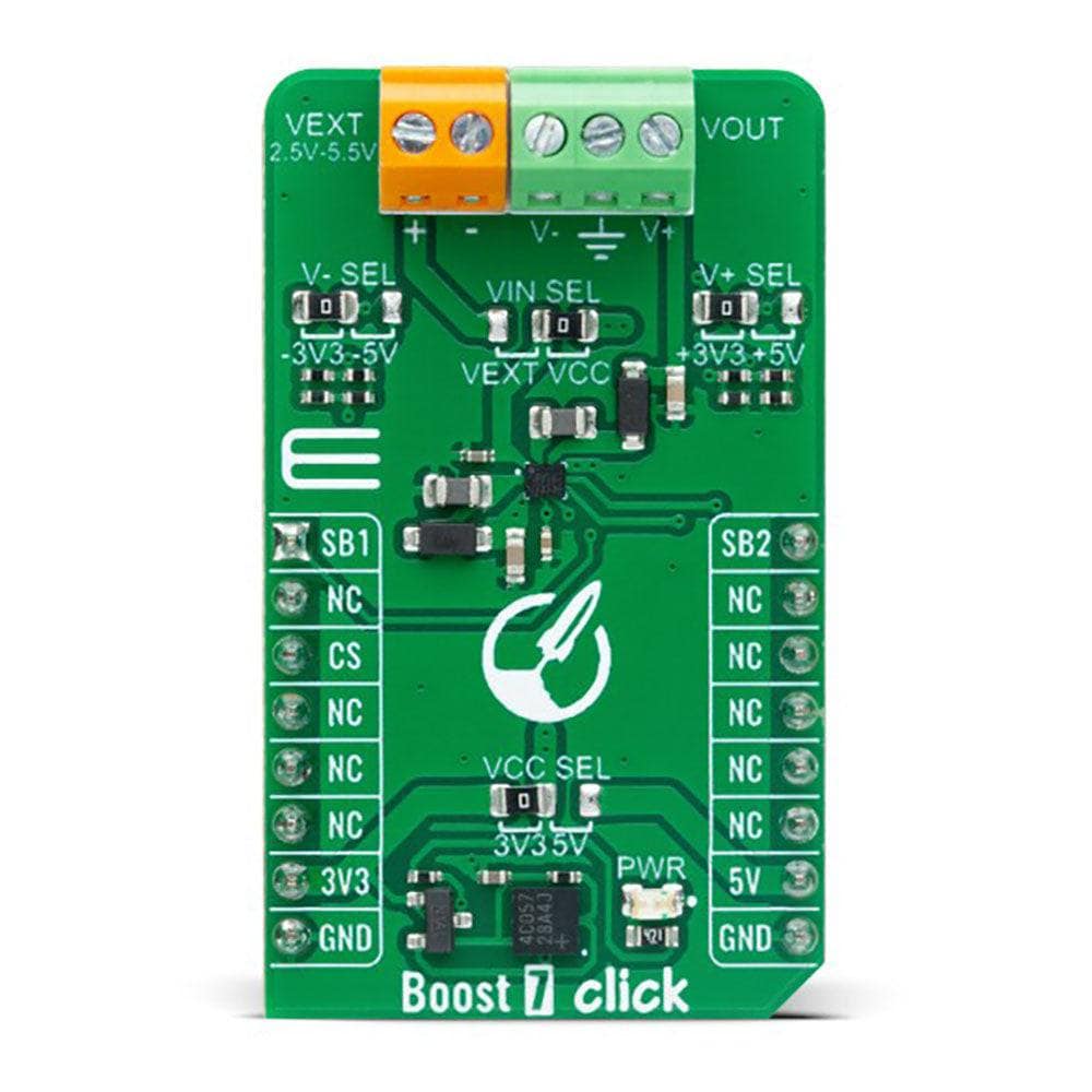
As mentioned, the BD8316GWL can configure the positive and negative output voltage in the ±3.3V or ±5V range. The desired output voltage can be selected by positioning SMD jumpers labelled as V- SEL and V+ SEL to an appropriate position. It is also possible to control the activity of the output channels via two mikroBUS™ pins, SB1 and SB2 pins. These pins are routed to a default position of the AN and PWM pins of the mikroBUS™ socket. By setting these pins to a high logic state, we put the converter outputs to an active state, and regulated voltages are available at the output terminals. In the same way, setting these pins to a low logic level disables the channels.
The Boost 7 Click Board™ can operate with either 3.3V or 5V logic voltage levels selected via the VCC SEL jumper. This way, both 3.3V and 5V capable MCUs can use the communication lines properly. Additionally, there is a possibility for the BD8316GWL power supply selection via jumper labelled as VIN SEL to supply the BD8316GWL from an external power supply terminal in the range from 2.5V to 5.5V or with a selected voltage from mikroBUS™ power rails. However, the Click board™ comes equipped with a library containing easy-to-use functions and an example code that can be used, as a reference, for further development.
SPECIFICATIONS
| Type | Boost |
| Applications | Can be used to step up an input voltage to some higher level |
| On-board modules | BD8316GWL - dual DC/DC converter from Rohm Semiconductor |
| Key Features | Regulated negative and positive outputs, current-limited, high efficiency, low power consumption, selectable converter power supply, digitally-controlled output channels, and more |
| Interface | GPIO |
| Compatibility | mikroBUS |
| Click board size | M (42.9 x 25.4 mm) |
| Input Voltage | 3.3V or 5V,External |
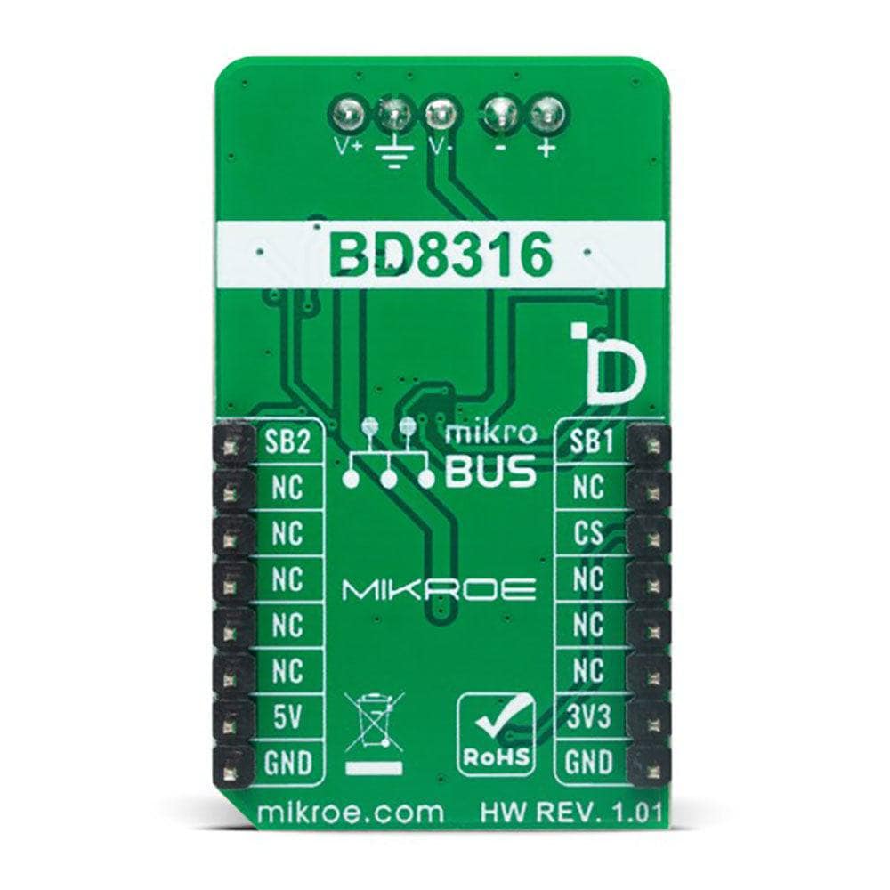
PINOUT DIAGRAM
This table shows how the pinout of the Boost 7 Click Board™ corresponds to the pinout on the mikroBUS™ socket (the latter shown in the two middle columns).
| Notes | Pin | Pin | Notes | ||||
|---|---|---|---|---|---|---|---|
| Negative Channel Control | SB1 | 1 | AN | PWM | 16 | SB2 | Positive Channel Control |
| NC | 2 | RST | INT | 15 | NC | ||
| NC | 3 | CS | RX | 14 | NC | ||
| NC | 4 | SCK | TX | 13 | NC | ||
| NC | 5 | MISO | SCL | 12 | NC | ||
| NC | 6 | MOSI | SDA | 11 | NC | ||
| Power Supply | 3.3V | 7 | 3.3V | 5V | 10 | 5V | Power Supply |
| Ground | GND | 8 | GND | GND | 9 | GND | Ground |
ONBOARD SETTINGS AND INDICATORS
| Label | Name | Default | Description |
|---|---|---|---|
| LD1 | PWR | - | Power LED Indicator |
| JP1 | V-SEL | Left | Negative Output Voltage Selection -3.3V/-5V: Left position -3.3V, Right position -5V |
| JP2 | V+SEL | Left | Positive Output Voltage Selection +3.3V/+5V: Left position +3.3V, Right position +5V |
| JP3 | VCC SEL | Left | Logic Level Voltage Selection 3V3/5V: Left position 3V3, Right position 5V |
| JP4 | VIN SEL | Right | BD8316GWL Power Supply Selection VEXT/VCC: Left position VEXT, Right position VCC |
BOOST 7 CLICK ELECTRICAL SPECIFICATIONS
| Description | Min | Typ | Max | Unit |
|---|---|---|---|---|
| Supply Voltage | 3.3 | - | 5 | V |
| External Supply Voltage | 2.5 | - | 5.5 | V |
| Positive Output Voltage | - | +3.3/+5 | - | V |
| Negative Output Voltage | - | -3.3/-5 | - | V |
| General Information | |
|---|---|
Part Number (SKU) |
MIKROE-5575
|
Manufacturer |
|
| Physical and Mechanical | |
Weight |
0.02 kg
|
| Other | |
EAN |
8606027385599
|
Frequently Asked Questions
Have a Question?
-
Is the Boost 7 Click Board™ ready to use?
Yes, the Boost 7 Click Board™ comes as a fully tested product, ready to be used on a system equipped with the mikroBUS™ socket.
-
What is the mikroSDK-compliant library for the Boost 7 Click Board™?
The Boost 7 Click Board™ is supported by a mikroSDK-compliant library, which includes functions that simplify software development.
-
What are the applications of the Boost 7 Click Board™?
The Boost 7 Click Board™ is used to step up an input voltage to some higher level required by a load, for various applications that require "split rail" operating voltages.
-
What is the voltage range of the external power supply that can be used with the Boost 7 Click Board™?
The Boost 7 Click Board™ provides the opportunity of using an external power supply with a very low voltage of 2.5V.
-
What is the current limit of each converter inside the BD8316GWL?
Each converter inside the BD8316GWL is designed with up to 200mA current limit.
-
What is the Boost 7 Click Board™?
The Boost 7 Click Board™ is an add-on board that steps up the voltage from its input (supply) to its output (load). It features the BD8316GWL, a dual DC/DC converter from Rohm Semiconductor, which is designed to generate well-regulated positive and negative outputs of ±3.3V or ±5V.