


Mikroelektronika d.o.o.
Clock Gen 4 Click Board™
Clock Gen 4 Click Board™
SKU: MIKROE-4300
Couldn't load pickup availability


Overview
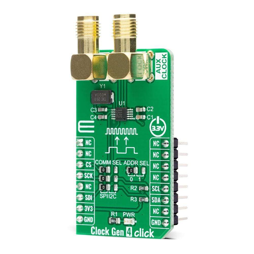
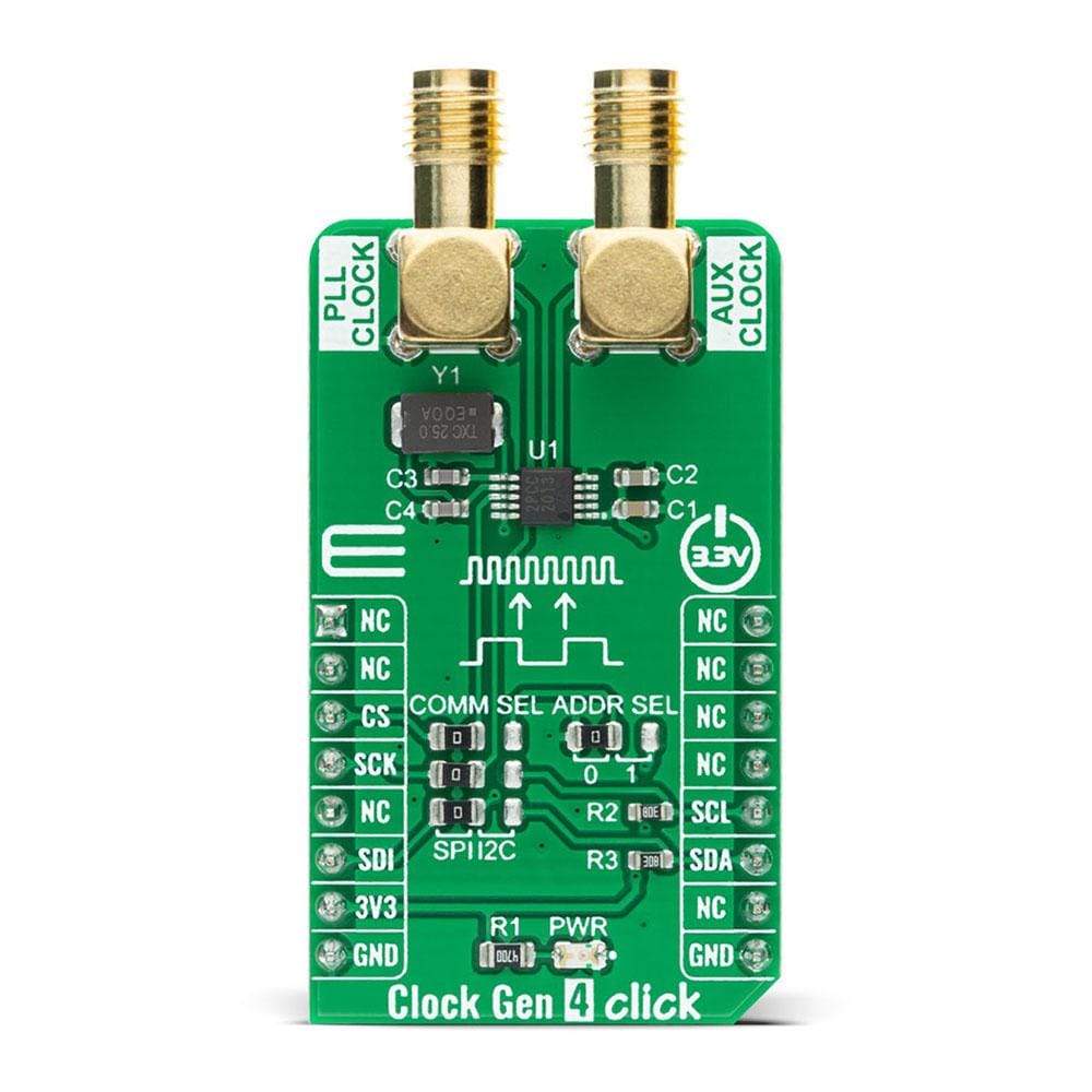
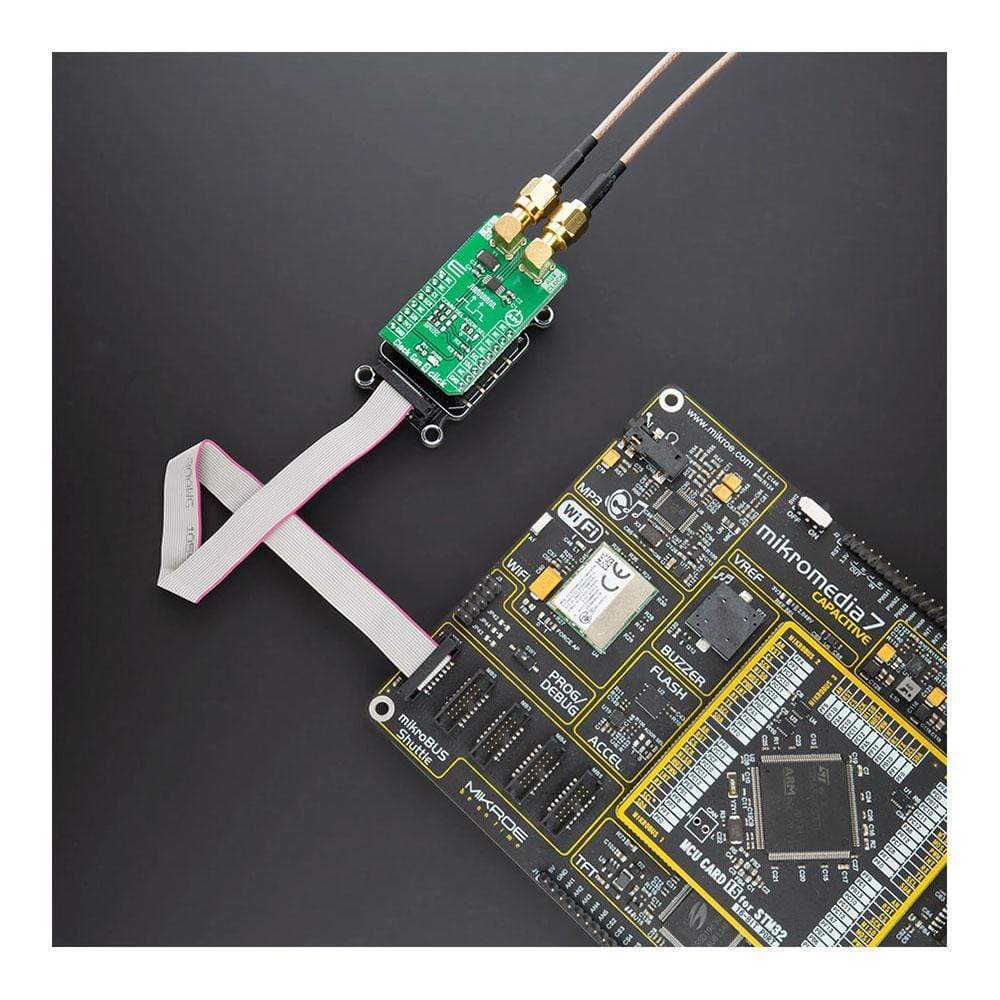
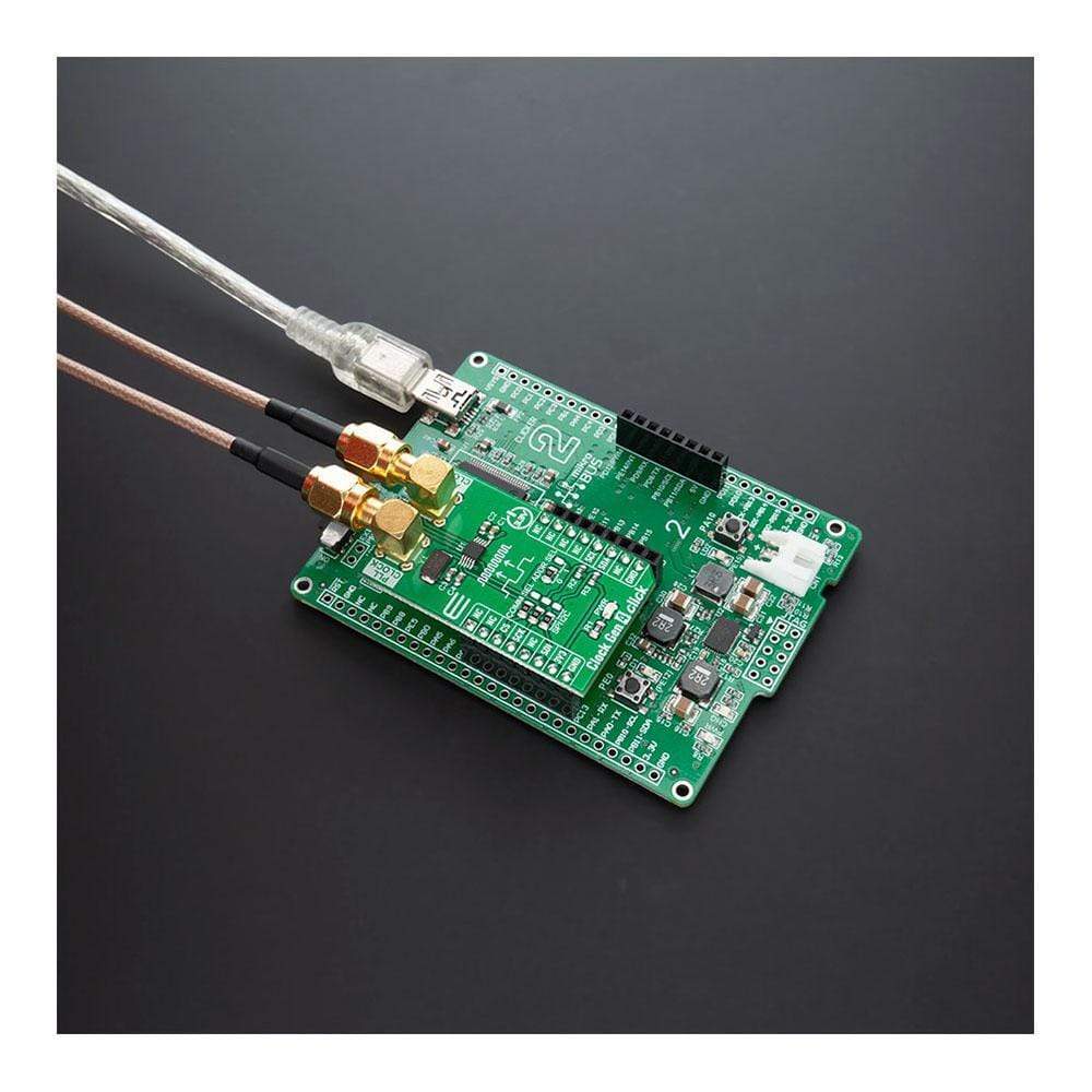
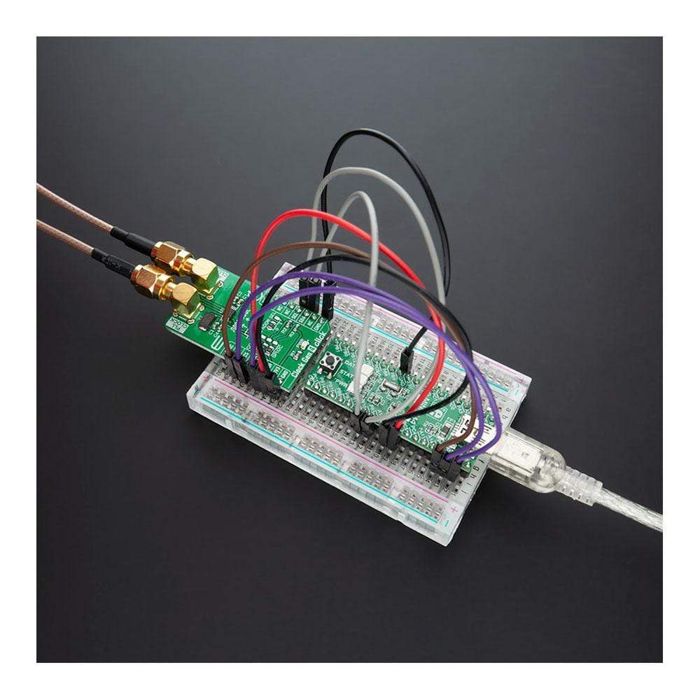
The Clock Gen 4 Click Board™ is a compact add-on board that contains both a clock generator and a multiplier/jitter reduced clock frequency synthesizer. This board features the CS2200-CP, an analogue PLL architecture comprised of a Delta-Sigma fractional-N frequency synthesizer from Cirrus Logic. This clocking device utilizes a programmable phase lock loop and allows frequency synthesis and clock generation from a stable reference clock. It generates a low-jitter PLL clock from an external crystal, supports both I²C and SPI for full software control, and also has configurable auxiliary clock output. This Click Board™ is suitable for MCU clock source, or in applications like digital effects processors, digital mixing consoles, and many more.
The Clock Gen 4 Click Board™ is supported by a mikroSDK compliant library, which includes functions that simplify software development. This Click Board™ comes as a fully tested product, ready to be used on a system equipped with the mikroBUS™ socket.
Downloads
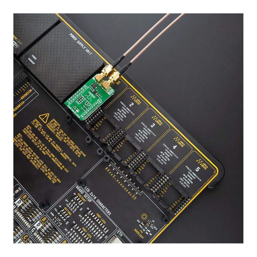
How Does The Clock Gen 4 Click Board™ Work?
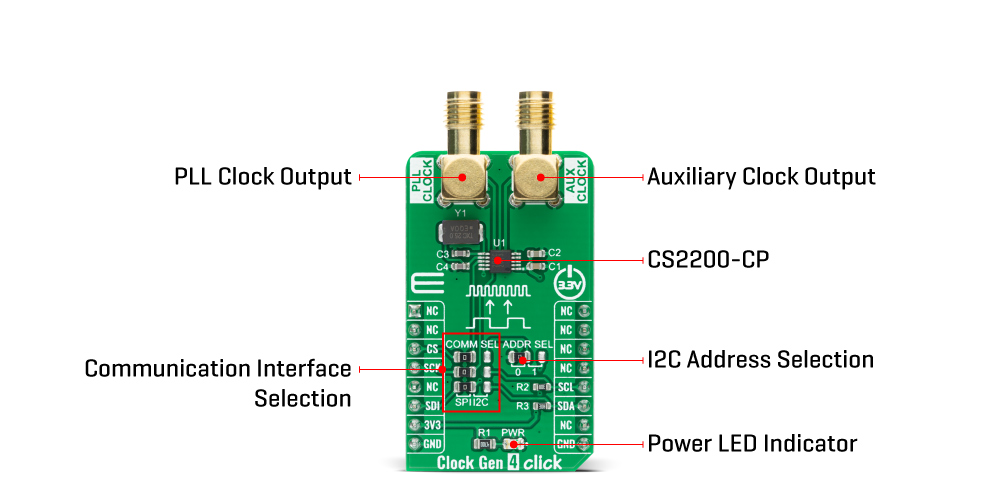
The Clock Gen 4 Click Board™ is based on the CS2200-CP, an analog PLL architecture comprised of a Delta-Sigma fractional-N frequency synthesizer from Cirrus Logic. The Delta-Sigma fractional-N frequency synthesizer has a very high resolution for Input/Output clock ratios, low phase noise, a wide range of output frequencies, and the ability to quickly tune to a new frequency. This synthesizer multiplies the timing reference clock by the value of N to generate a stable and low-jitter PLL clock available on the connector labeled as PLL Clock. The Clock Gen 4 Click Board™ also has another connector marked as AUX Clock that outputs a buffered version of one of the input/output clocks, or a status signal, depending on register configuration.
The analog PLL based frequency synthesizer uses a low-jitter timing reference clock as time and phase reference for the internal voltage controlled oscillator (VCO). The phase comparator compares the fractional-N divided clock with the original timing reference and generates a control signal that is filtered by the internal loop filter to generate the VCO's control voltage that sets its output frequency. The Delta-Sigma modulator modulates the loop integer divide ratio to get the desired fractional ratio between the reference clock and the VCO output. This allows fast lock times for a wide range of output frequencies without the need for external filter components.
The Clock Gen 4 Click Board™ provides the possibility of using both I2C and SPI interfaces with a maximum frequency of 100 kHz for I2C and 6 MHz for SPI communication. The selection can be performed by positioning SMD jumpers labeled as COMM SEL to an appropriate position. Note that all the jumpers must be placed to the same side, or else the Click board™ may become unresponsive. While the I2C interface is selected, the CS2200-CP allows the choice of the least significant bit (LSB) of its I2C slave address. This can be done by using the SMD jumper labeled as ADDR SEL.
The Clock Gen 4 Click Board™ is designed to be operated only with a 3.3V logic voltage level. A proper logic voltage level conversion should be performed before the Click board™ is used with MCUs with different logic levels. However, the Click board™ comes equipped with a library that contains easy to use functions and an example code that can be used as a reference for further development.
SPECIFICATIONS
| Type | Clock generator |
| Applications | Can be used as an MCU clock source, or in applications like digital effects processors, digital mixing consoles, and many more. |
| On-board modules | Clock Gen 4 Click is based on the CS2200-CP, an analog PLL architecture comprised of a Delta-Sigma fractional-N frequency synthesizer from Cirrus Logic. |
| Key Features | High-performance analog/digital phase locked loop, clock generation/frequency synthesis and multiplier/jitter reduction, flexible control options, configurable auxiliary output, and more. |
| Interface | I2C,SPI |
| Compatibility | mikroBUS |
| Click board size | M (42.9 x 25.4 mm) |
| Input Voltage | 3.3V |
PINOUT DIAGRAM
This table shows how the pinout on the Clock Gen 4 Click Board™ corresponds to the pinout on the mikroBUS™ socket (the latter shown in the two middle columns).
| Notes | Pin | Pin | Notes | ||||
|---|---|---|---|---|---|---|---|
| NC | 1 | AN | PWM | 16 | NC | ||
| NC | 2 | RST | INT | 15 | NC | ||
| SPI Chip Select | CS | 3 | CS | RX | 14 | NC | |
| SPI Clock | SCK | 4 | SCK | TX | 13 | NC | |
| SPI Data OUT | SDO | 5 | MISO | SCL | 12 | SCL | I2C Clock |
| SPI Data IN | SDI | 6 | MOSI | SDA | 11 | SDA | I2C Data |
| Power Supply | 3.3V | 7 | 3.3V | 5V | 10 | NC | |
| Ground | GND | 8 | GND | GND | 9 | GND | Ground |
ONBOARD SETTINGS AND INDICATORS
| Label | Name | Default | Description |
|---|---|---|---|
| LD1 | PWR | - | Power LED Indicator |
| JP1-JP3 | COMM SEL | Left | Communication Interface Selection: Left position SPI, Right position I2C |
| JP4 | ADDR SEL | Left | I2C Address Selection: Left position 0, Right position 1 |
| CN1 | PLL | - | PLL Clock Output SMA Connector |
| CN2 | AUX | - | Auxiliary Clock Output SMA Connector |
CLOCK GEN 4 CLICK ELECTRICAL SPECIFICATIONS
| Description | Min | Typ | Max | Unit |
|---|---|---|---|---|
| Supply Voltage | 3.1 | 3.3 | 3.5 | V |
| PLL Clock Output Frequency | 6 | - | 75 | MHz |
| Output Frequency Synthesis Resolution | 0 | - | ±0.5 | ppm |
| Operating Temperature Range | -10 | - | +70 | °C |
| General Information | |
|---|---|
Part Number (SKU) |
MIKROE-4300
|
Manufacturer |
|
| Physical and Mechanical | |
Weight |
0.023 kg
|
| Other | |
EAN |
8606027380877
|
Frequently Asked Questions
Have a Question?
Be the first to ask a question about this.