


Mikroelektronika d.o.o.
Expand 7 Click Board™
Expand 7 Click Board™
SKU: MIKROE-4244
Couldn't load pickup availability
Key Features
Overview
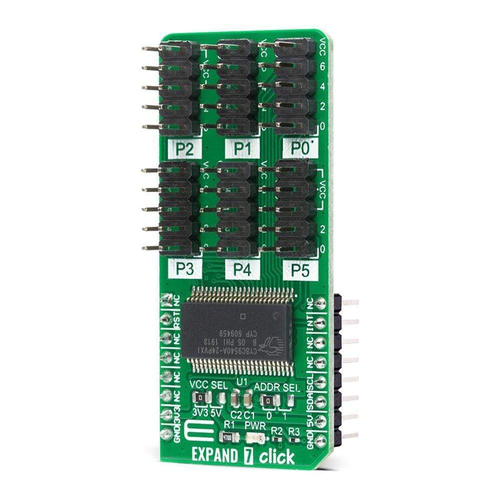
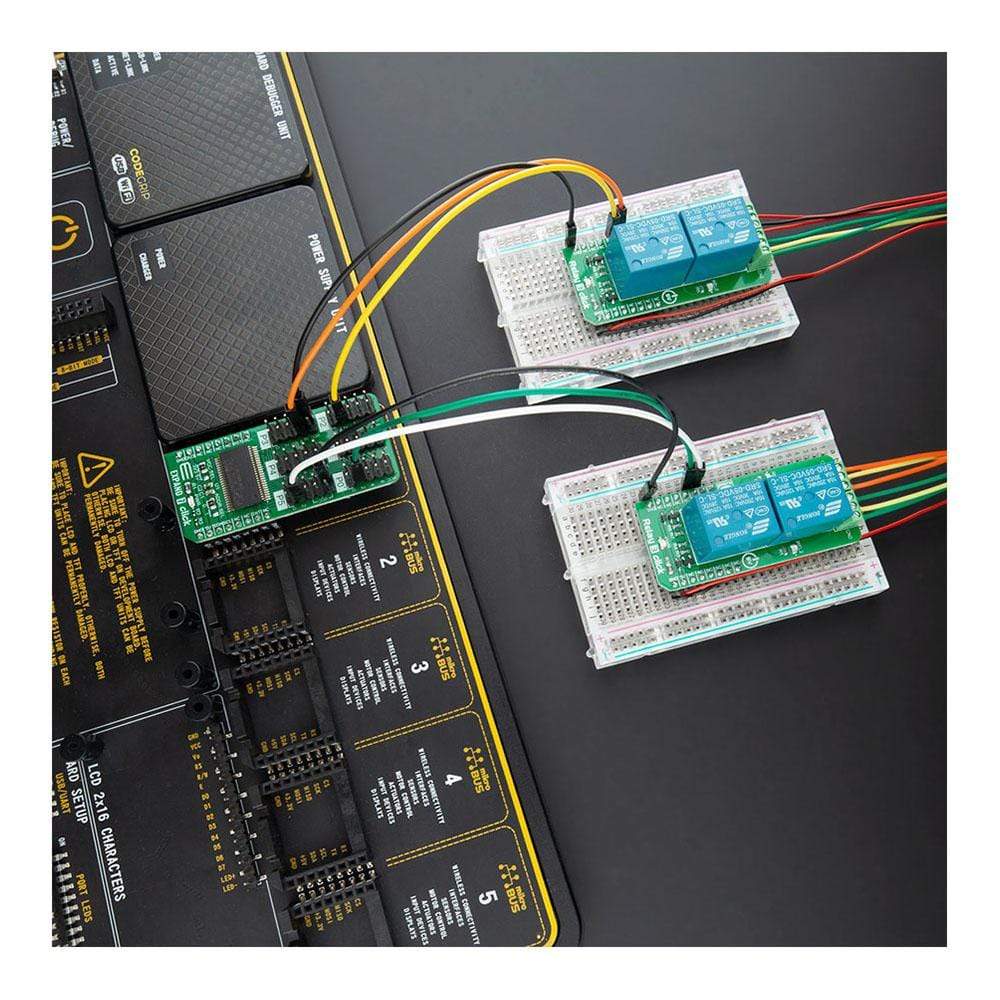
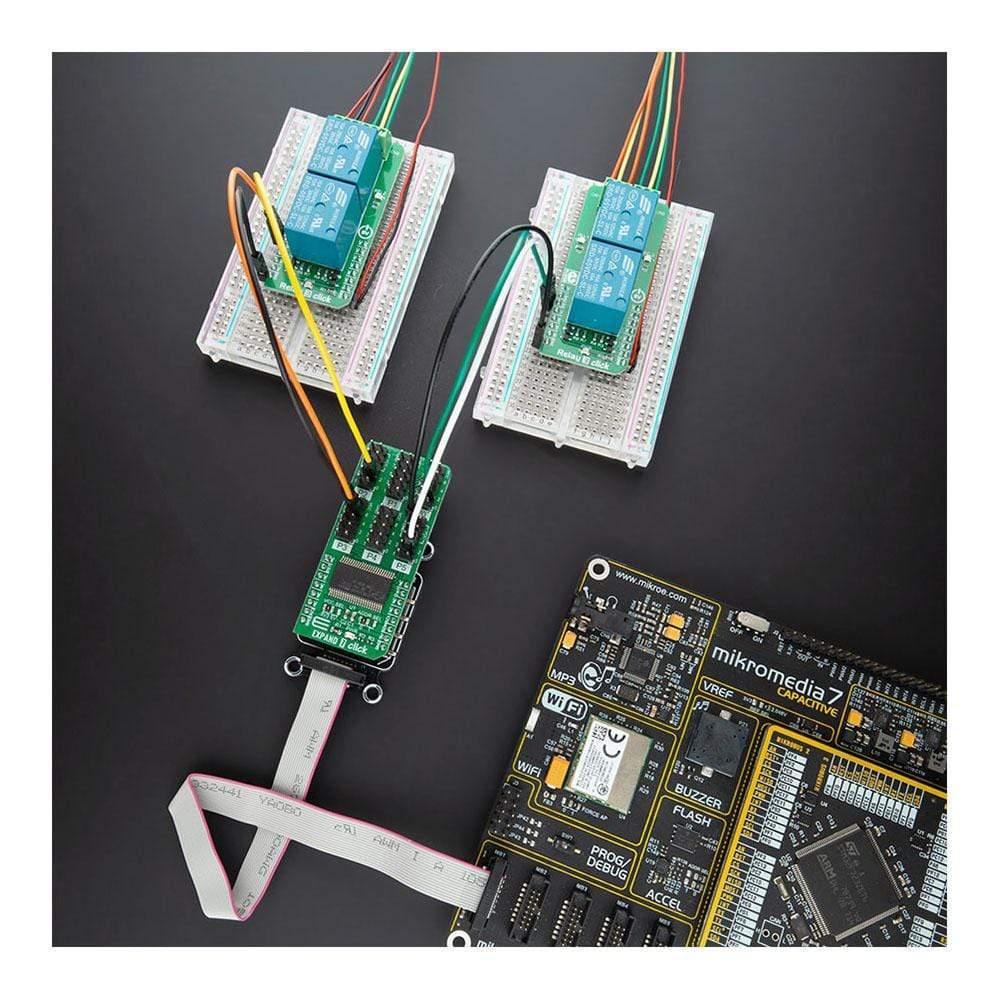
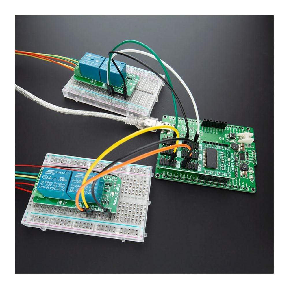
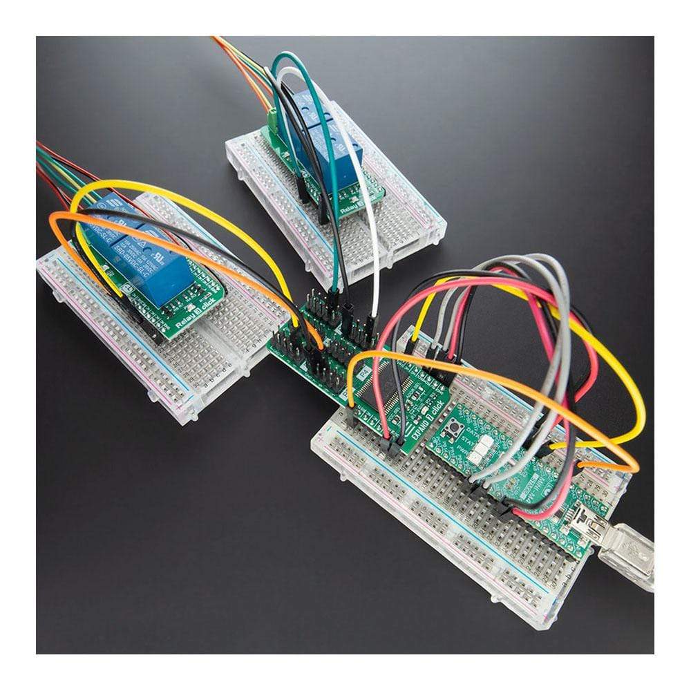
The Expand 7 Click Board™ is a compact add-on board that contains a multi-port I/O expander with bi-directional input/outputs or PWM outputs. This board features the CY8C9540A, 40-bit I/O port expander with EEPROM and 8 independently configurable 8-bit PWM outputs from Cypress Semiconductor. The CY8C9540A operates as two I2C slave devices, first as a multi-port I/O expander, and second as a serial EEPROM with 11 Kbyte address space. It has a user default storage, flexible I2C address configuration, and a programmable interrupt and reset function. This Click Board™ can be used to monitor and control LEDs and system intrusion detection devices, but also as a storage for information such as error codes or board manufacturing data for diagnostic purposes.
The Expand 7 Click is supported by a mikroSDK compliant library, which includes functions that simplify software development. This Click Board™ comes as a fully tested product, ready to be used on a system equipped with the mikroBUS™ socket.
Downloads
How Does The Expand 7 Click Board™ Work?
The Expand 7 Click Board™ is based on the CY8C9540A, 40-bit I/O expander with EEPROM, and 8 independently configurable 8-bit PWM outputs from Cypress Semiconductor. The main blocks of the CY8C9540A include the control unit, PWMs, EEPROM, and I/O ports. The I/O expander's data pins can be independently assigned as inputs, outputs, or PWM outputs, and can be configured as open-drain or collector, strong drive (10 mA source, 25 mA sink), resistively pulled up or down, or high impedance which can be selected in the Port Drive Mode register. It operates as two I2C slave devices, where the first device is a multi-port I/O expander (single I2C address to access all ports through registers), and the second device is a serial EEPROM with 11 Kbyte address space.
.jpg)
Configuration and output register settings are storable as user defaults in a dedicated section of the EEPROM. If user defaults were stored in EEPROM, they are restored to the ports at Power-Up. The EEPROM is byte readable and supports byte-by-byte writing. A pin 3 of the Port 2 on this Click board™ can be configured as an EEPROM Write Disable (WD) input that blocks write operations when set high. The configuration registers can also disable EEPROM operations.
EXPAND 7 Click communicates with MCU using the standard I2C 2-Wire interface with a maximum frequency of 100kHz. The CY8C9540A has, by default, two possible I2C slave address formats: the first is used to access the multi-port device, and the second to access the EEPROM. This selection of I2C slave addresses is performed by setting the logic level on the A0 pin of the CY8C9540A which can be done by using the SMD jumper labeled as ADDR SEL.
It also generates a programmable interrupt signal routed on the INT pin of the mikroBUS™, which can inform the system master that there is incoming data on its ports or that the PWM output state was changed. The reset signal routed on the RST pin of the mikroBUS™ socket is similar to POR (Power-ON Reset) function. When the CY8C9540A is held in Reset, all In and Out pins are held at their default High-Z State.
This Click board™ is designed to be operated with both 3.3V and 5V logic voltage levels that can be selected via VCC SEL jumper. This allows for both 3.3V and 5V capable MCUs to use the I2C communication lines properly. More information about the CY8C9540A can be found in the attached datasheet. However, the Click board™ comes equipped with a library that contains easy to use functions and a usage example that may be used as a reference for further development.
SPECIFICATIONS
| Type | Port expander |
| Applications | Can be used to monitor and control LEDs and system intrusion detection devices, but also as a storage for information such as error codes or board manufacturing data for diagnostic purposes. |
| On-board modules | EXPAND 7 Click is based on the CY8C9540A, 40-bit I/O expander with EEPROM, and 8 independently configurable 8-bit PWM outputs from Cypress Semiconductor. |
| Key Features | 20-bit, 100kHz I2C port expander, flexible I2C address configuration, internal 3Kbyte EEPROM, user default storage, and more. |
| Interface | I2C |
| Compatibility | mikroBUS |
| Click board size | L (57.15 x 25.4 mm) |
| Input Voltage | 3.3V or 5V |
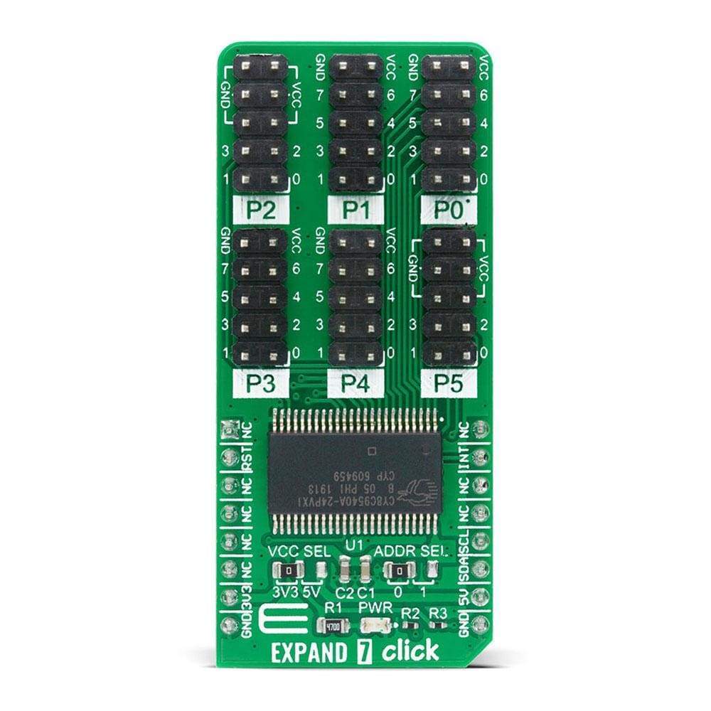
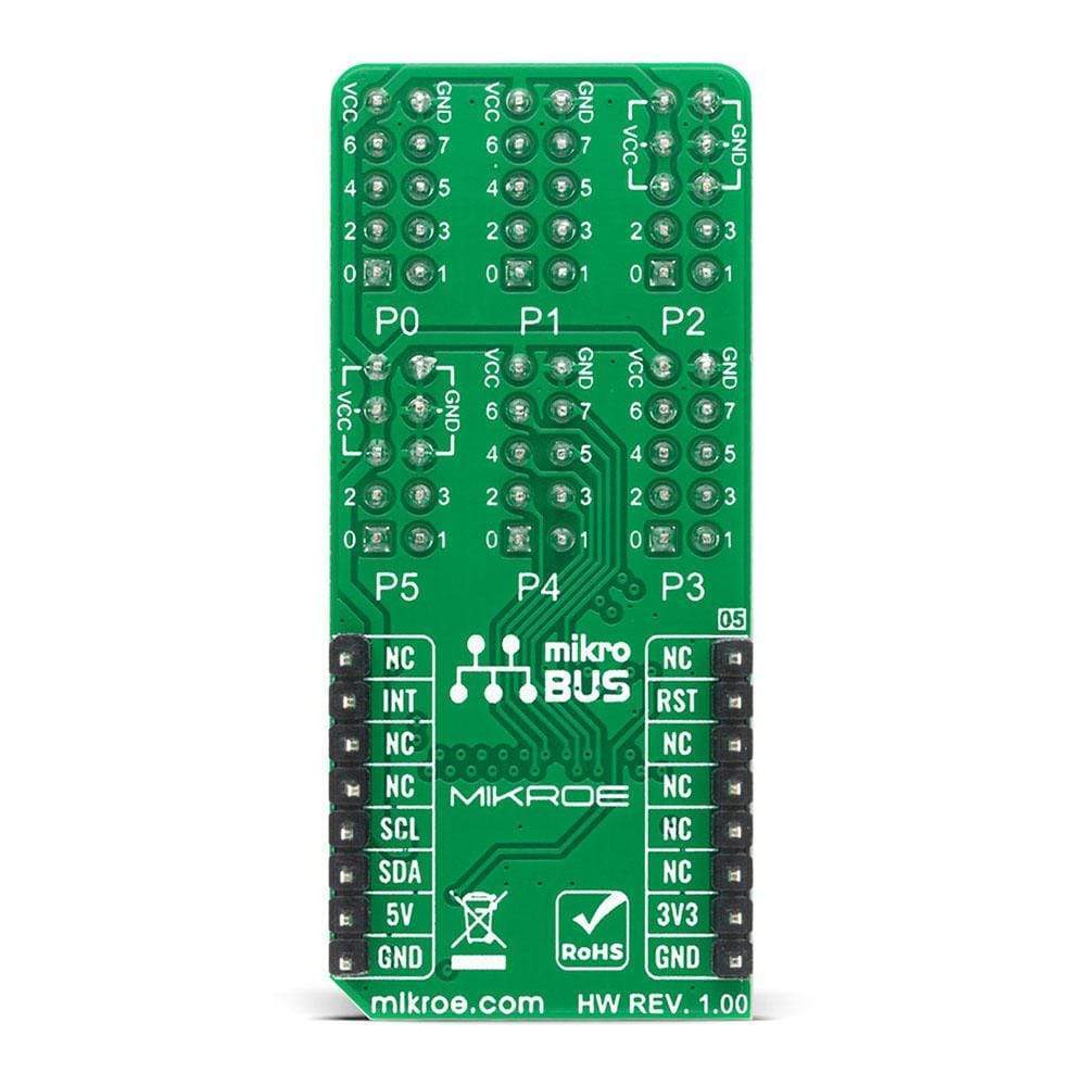
PINOUT DIAGRAM
This table shows how the pinout on EXPAND 7 Click corresponds to the pinout on the mikroBUS™ socket (the latter shown in the two middle columns).
| Notes | Pin | Pin | Notes | ||||
|---|---|---|---|---|---|---|---|
| NC | 1 | AN | PWM | 16 | NC | ||
| Reset | RST | 2 | RST | INT | 15 | INT | Interrupt |
| NC | 3 | CS | RX | 14 | NC | ||
| NC | 4 | SCK | TX | 13 | NC | ||
| NC | 5 | MISO | SCL | 12 | SCL | I2C Clock | |
| NC | 6 | MOSI | SDA | 11 | SDA | I2C Data | |
| Power Supply | 3.3V | 7 | 3.3V | 5V | 10 | 5V | Power Supply |
| Ground | GND | 8 | GND | GND | 9 | GND | Ground |
ONBOARD SETTINGS AND INDICATORS
| Label | Name | Default | Description |
|---|---|---|---|
| LD1 | PWR | - | Power LED Indicator |
| JP1 | VCC SEL | Left | Power Supply Voltage Selection 3V3/5V: Left position 3V3, Right position 5V |
| JP2 | ADDR SEL | Left | Communication interface selection: Left position 0, Right position 1 |
| J1-J6 | P0-P5 Port | - | I/O Expander Ports |
EXPAND 7 CLICK ELECTRICAL SPECIFICATIONS
| Description | Min | Typ | Max | Unit |
|---|---|---|---|---|
| Supply Voltage | -0.5 | - | 6 | V |
| High Level Source Current | 10 | - | - | mA |
| Low Level Sink Current | 25 | - | - | mA |
| Operating Temperature Range | -40 | - | +85 | °C |
| General Information | |
|---|---|
Part Number (SKU) |
MIKROE-4244
|
Manufacturer |
|
| Physical and Mechanical | |
Weight |
0.024 kg
|
| Other | |
EAN |
8606027380464
|
Frequently Asked Questions
Have a Question?
Be the first to ask a question about this.