


Mikroelektronika d.o.o.
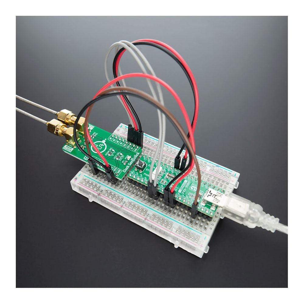
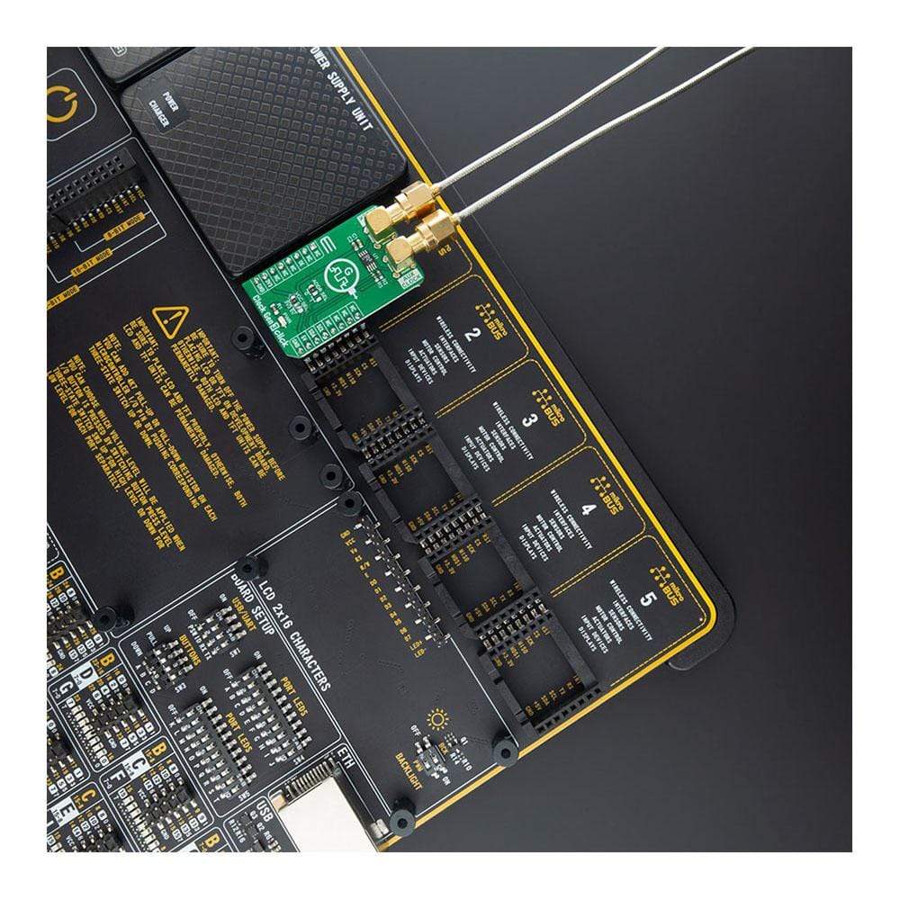
Clock Gen 3 Click Board™
Clock Gen 3 Click Board™
SKU: MIKROE-4171
Couldn't load pickup availability


Overview
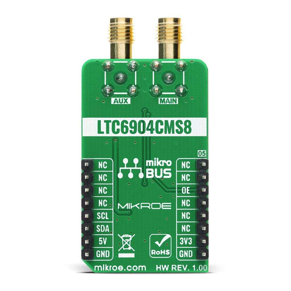
The Clock Gen 3 Click Board™ features a low power self-contained digital frequency source providing a precision frequency from 1kHz to 68MHz, set through a serial port. The Clock Gen 3 Click Board™, an I2C configurable clock generator, features the LTC6904 from Analog Devices and requires no external components other than a power supply bypass capacitor, and it operates over a single wide supply voltage range of 2.7V to 5.5V. The LTC6904 features a proprietary feedback loop that linearizes the relationship between digital control settings and frequency.
It has many features that make it attractive for various applications such as a microcontroller clock source, clock source for a switched capacitor filter, or general replacement for a DAC/VCO combination.
Downloads
How Does The Clock Gen 3 Click Board™ Work?
The Clock Gen 3 Click Board™ uses the LTC6904 IC, 1kHz to 68MHz Serial Port Programmable Oscillator from Linear Technology. The LTC6904 is a low power self-contained digital frequency source providing a precision frequency from 1KHz to 68MHz, which is set by the I2C interface operaing up to 3.4 Mbps. This Click board™ features on-board I2C address jumpers, pull-up resistors, a power supply bypass capacitor, and a power LED. The maximum frequency error is 1.1% or 1.6% when operating with a flexible power supply voltage range from 2.7V to 5V, which makes it suitable for 3.3V and 5V MCUs.
.jpg)
In most frequency ranges, the output of the Clock Gen 3 Click Board™ is generated as a division of the higher internal clock frequency. This helps to minimize jitter and subharmonics at the output of the device. In the highest frequency ranges, the division ratio is reduced, which will result in a greater cycle-to-cycle jitter as well as spurs at the internal sampling frequency. Because the internal control loop runs at 1MHz to 2MHz without regard to the output frequency, output spurs separated from the set frequency by 1MHz to 2MHz may be observed. These spurs are characteristically more than 30dB below the level of the set frequency.
The LTC6904 communicates with the MCU using the standard I2C 2-wire interface. The two bus lines, SDA and SCL, must be HIGH when the bus is not in use. If the I2C interface is not driven with a standard I2C compatible device, care must be taken to ensure that the SDA line is released during the ACK cycle to prevent bus contention. The LTC6904 can respond to one of two 7-bit addresses. The first 6 bits (MSBs) have been factory programmed to 001011. The address pin, ADR (Pin 4) is programmed by the user and determines the LSB of the slave address and it can be selected by an onboard SMD jumper labeled as ADD SEL allowing selection of the slave address LSB.
The Clock Gen 3 Click Board™ can be supplied and interfaced with both 3.3V and 5V without the need for any external components. The onboard SMD jumper labeled as VCC SEL allows voltage selection for interfacing with both 3.3V and 5V microcontrollers. More information about the LTC6904 can be found in the attached datasheet. However, this Click board™ comes equipped with a library that contains easy to use functions and an example that may be used as a reference for development.
SPECIFICATIONS
| Type | Clock generator |
| Applications | Can be used as a microcontroller clock source, clock source for a switched capacitor filter, or general replacement for a DAC/VCO combination. |
| On-board modules | LTC6904 |
| Key Features | Precision frequency generator from 1KHz to 68MHz, minimal jitter and subharmonics at the output, on-board I2C address jumpers |
| Interface | GPIO,I2C |
| Compatibility | mikroBUS |
| Click board size | M (42.9 x 25.4 mm) |
| Input Voltage | 3.3V,5V |
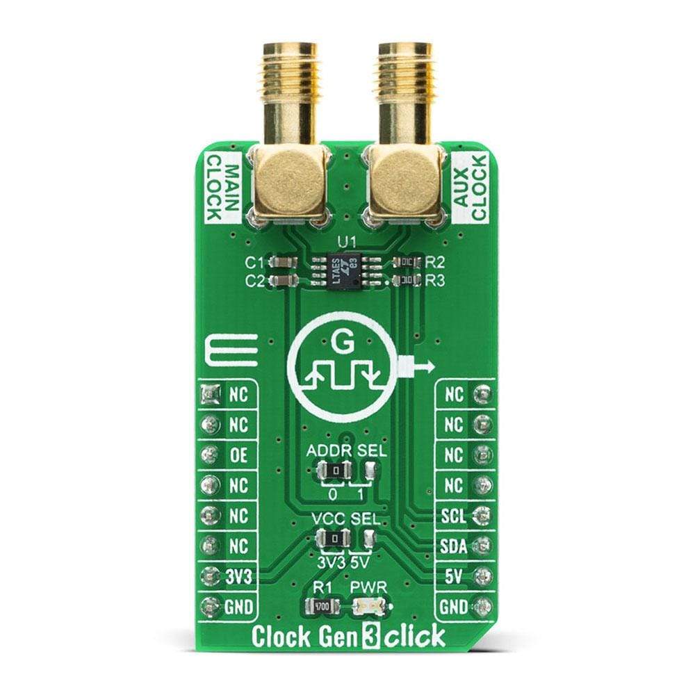
PINOUT DIAGRAM
This table shows how the pinout on the Clock Gen 3 Click Board™ corresponds to the pinout on the mikroBUS™ socket (the latter shown in the two middle columns).
| Notes | Pin | Pin | Notes | ||||
|---|---|---|---|---|---|---|---|
| NC | 1 | AN | PWM | 16 | NC | ||
| NC | 2 | RST | INT | 15 | NC | ||
| Output Enable | OE | 3 | CS | RX | 14 | NC | |
| NC | 4 | SCK | TX | 13 | NC | ||
| NC | 5 | MISO | SCL | 12 | SCL | I2C Clock | |
| NC | 6 | MOSI | SDA | 11 | SDA | I2C Data | |
| Power Supply | 3.3V | 7 | 3.3V | 5V | 10 | 5V | Power Supply |
| Ground | GND | 8 | GND | GND | 9 | GND | Ground |
ONBOARD SETTINGS AND INDICATORS
| Label | Name | Default | Description |
|---|---|---|---|
| LD1 | PWR | - | Power LED Indicator |
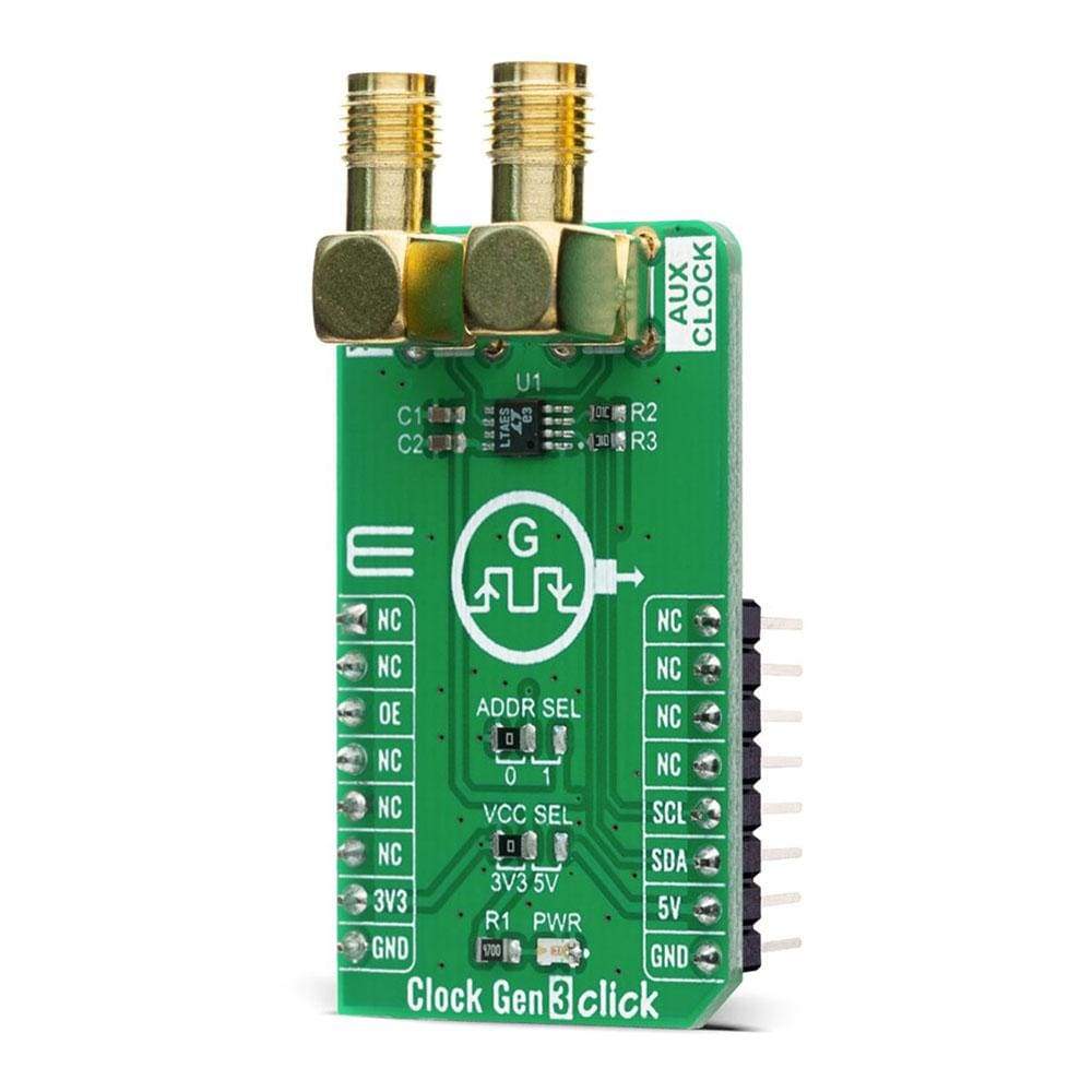
| JP1 | VCC SEL | Right | Power Supply Voltage Selection 3V3/5V, left position 3V3, right position 5V |
| JP2 | ADDR SEL | Left | I2C Address Selection: Left position 0, Right position 1 |
| CN1 | CN1 | - | Main Clock Output SMA connector |
| CN2 | CN2 | - | Auxiliary Clock output SMA connector |
MAXIMUM RATINGS (LIMITING CONDITIONS)
| Description | Min | Typ | Max | Unit |
|---|---|---|---|---|
| Supply Voltage | 2.7 | - | 5.5 | V |
| SMBus Operating Frequency | 10 | - | 100 | kHz |
| Output Impedance | - | 50 | - | Ω |
| Operating Temperature Range | -40 | +25 | +85 | °C |
| General Information | |
|---|---|
Part Number (SKU) |
MIKROE-4171
|
Manufacturer |
|
| Physical and Mechanical | |
Weight |
0.023 kg
|
| Other | |
EAN |
8606018717958
|
Frequently Asked Questions
Have a Question?
Be the first to ask a question about this.