


Mikroelektronika d.o.o.
LLC-I2C Click Board™
LLC-I2C Click Board™
SKU: MIKROE-3276
Couldn't load pickup availability


Key Features
Overview
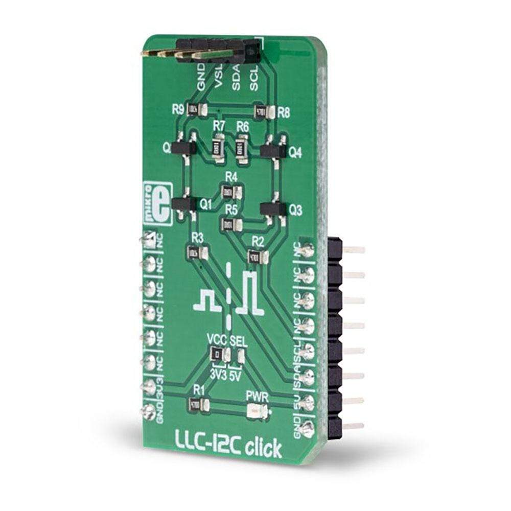
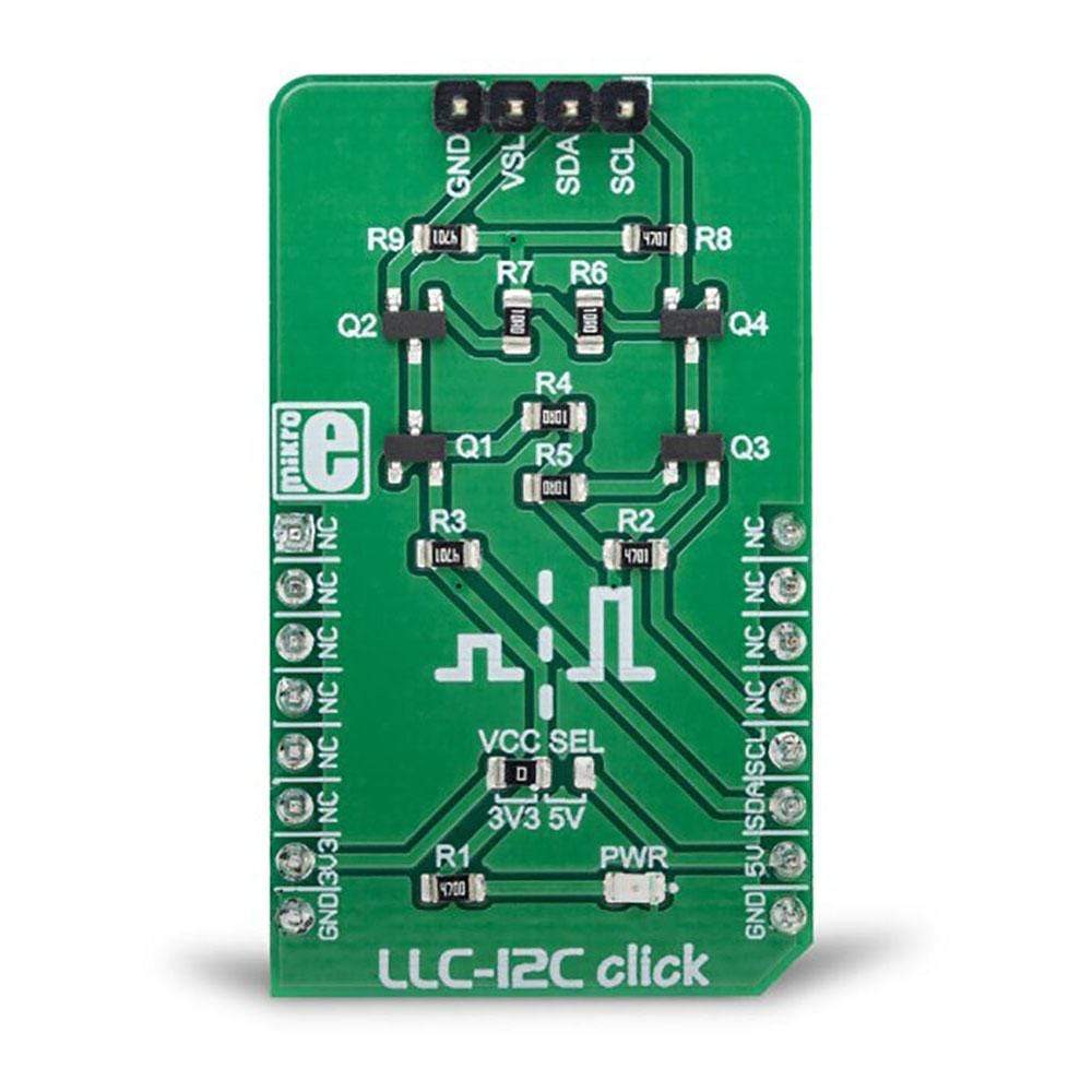
The LLC I2C Click Board™ can be utilized as the level converter for logic signals, which makes it a very useful Click Board™. The topology of this logic level conversion (LLC) circuit is perfectly suited for the bi-directional I2C communication. Although there are some specialised integrated circuits on the market, sometimes it is more convenient to have a simple solution made of just a few passive elements and four MOSFETs. Besides this, MOSFETs can withstand up to 20V across their terminals (12V VGS), and they support far greater currents than typical ICs, making them less likely to fail. The LLC circuitry, also known as the level translator or level shifter, can be used in virtually any application that utilizes the I2C communication protocol and needs matching between the logic voltage levels
Downloads
How Does The LLC I2C Click Board™ Work?
The LLC I2C Click Board™ does not use an integrated circuit, as already mentioned. With ICs avoided completely, there are some benefits gained: the overall cost of the LLC circuit is greatly reduced, a more robust MOSFET solution reduces the failure rate, and when powered off, both the low voltage and the high voltage sides are isolated from one another (by non-conductive MOSFETs). This type of circuit is sometimes referred to as a level shifting or level translating circuit and it is often necessary when the I2C slave device (typically a sensor IC) uses different logic voltage levels for the I2C communication than the master device, which is a host microcontroller in most cases. The conversion of this circuitry is bi-directional, which makes it suitable to be used with the I2C communication protocol.
The I2C protocol was first introduced by NXP Semiconductors (formerly Philips Semiconductors), in 1982. They also introduced an application note that explains the operation of the LLC circuit in more details. The circuit is divided into low-side and high-side sections for future reference, although the circuit is symmetrical and can be used in both directions.
When there is no communication going on, both gates and sources of the MOSFETs are pulled up to their specific reference voltage levels. This will turn OFF both MOSFETs since there is no gate-source voltage difference (e.g. VG=VS=VSL).
Since the I2C is operated by asserting its bus lines to a LOW logic level, when the source terminal of the MOSFET on one side (e.g. high-side) is driven to a LOW logic level, its VGS potential will rise since the gate voltage is fixed. When the VGS reaches the threshold voltage (1.2V typically for the used transistors), the MOSFET will turn ON, conducting current through the body diode of the opposite-side (low-side) MOSFET, which will become directly polarized. This mechanism can be used to convert signal levels in both directions, within the whole operating range of the used MOSFETs.
The reference voltage for the high-side can be selected by using the SMD jumper labelled as VCC SEL. The pull-up voltage for the high-side can be selected from the mikroBUS™ power rails, so it can be either 3.3V or 5V. For the low-side, an arbitrary reference voltage can be applied to the VSL pin of the J1 header, respecting the maximum voltage rating. J1 is the standard, 2.54mm pin-header. The low-side I2C bus pins are also routed to the J1 header, allowing an external device to be connected (using the standard wire-jumpers). As already mentioned, the low-side can actually use higher voltage levels than the master, but in most usage scenarios, it will be lower than the master, thus the terminology.
SPECIFICATIONS
| Type | Port expander |
| Applications | I2C logic level conversion circuit has its use in many different projects. It is used for the I2C logic voltage level matching between the slave and the master device |
| On-board modules | None |
| Key Features | Very low cost achieved using only passive elements, and four MOSFETs, ability to use an arbitrary voltage level conversion in the range from 1.2V up to 10V |
| Interface | I2C |
| Compatibility | mikroBUS |
| Click board size | M (42.9 x 25.4 mm) |
| Input Voltage | 3.3V or 5V |
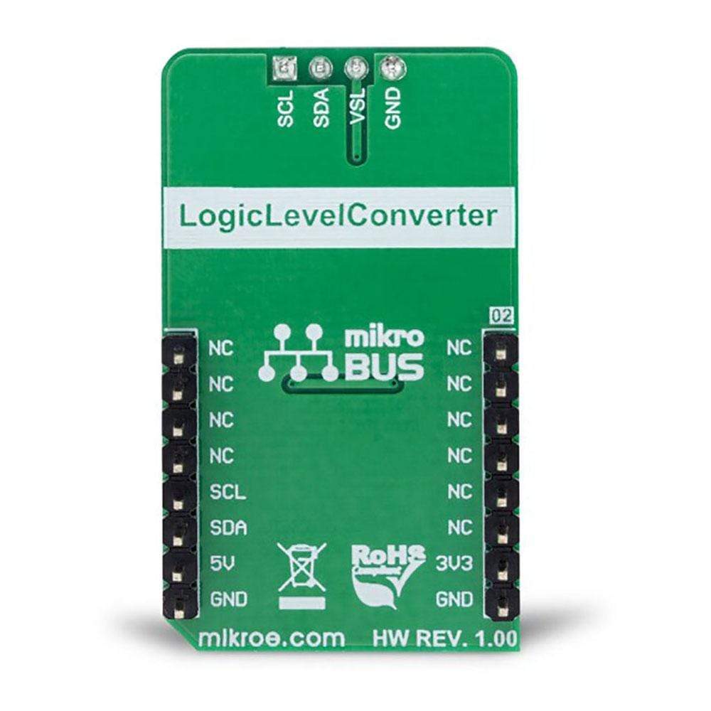
PINOUT DIAGRAM
This table shows how the pinout of the LLC I2C Click Board™ corresponds to the pinout on the mikroBUS™ socket (the latter shown in the two middle columns).
| Notes | Pin | Pin | Notes | ||||
|---|---|---|---|---|---|---|---|
| NC | 1 | AN | PWM | 16 | NC | ||
| NC | 2 | RST | INT | 15 | NC | ||
| NC | 3 | CS | RX | 14 | NC | ||
| NC | 4 | SCK | TX | 13 | NC | ||
| NC | 5 | MISO | SCL | 12 | SCL | I2C Clock | |
| NC | 6 | MOSI | SDA | 11 | SDA | I2C Data | |
| Power supply | 3V3 | 7 | 3.3V | 5V | 10 | 5V | Power supply |
| Ground | GND | 8 | GND | GND | 9 | GND | Ground |
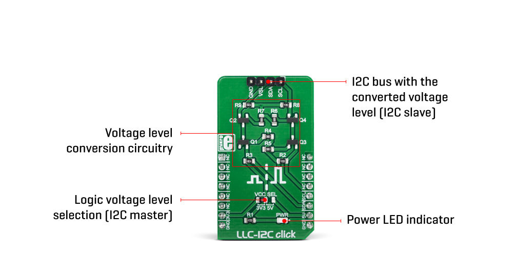
ONBOARD SETTINGS AND INDICATORS
| Label | Name | Default | Description |
|---|---|---|---|
| PWR | PWR | - | Power LED indicator |
| VCC SEL | VCC SEL | Left | Logic voltage level selection (master): left position 3.3V, right position 5V |
| J1 | - | - | I2C bus with the converted voltage levels (I2C slave) |
| General Information | |
|---|---|
Part Number (SKU) |
MIKROE-3276
|
Manufacturer |
|
| Physical and Mechanical | |
Weight |
0.019 kg
|
| Other | |
EAN |
8606018714049
|
Frequently Asked Questions
Have a Question?
Be the first to ask a question about this.