


Mikroelektronika d.o.o.
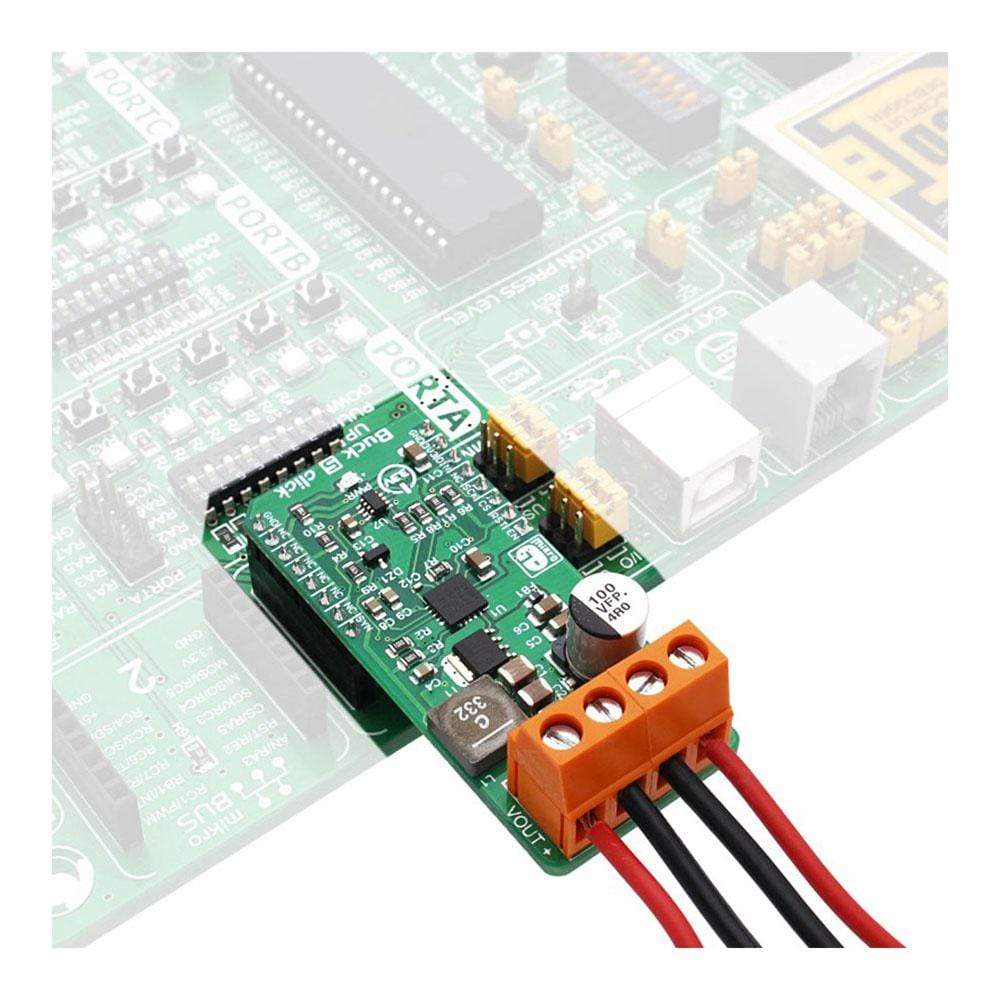
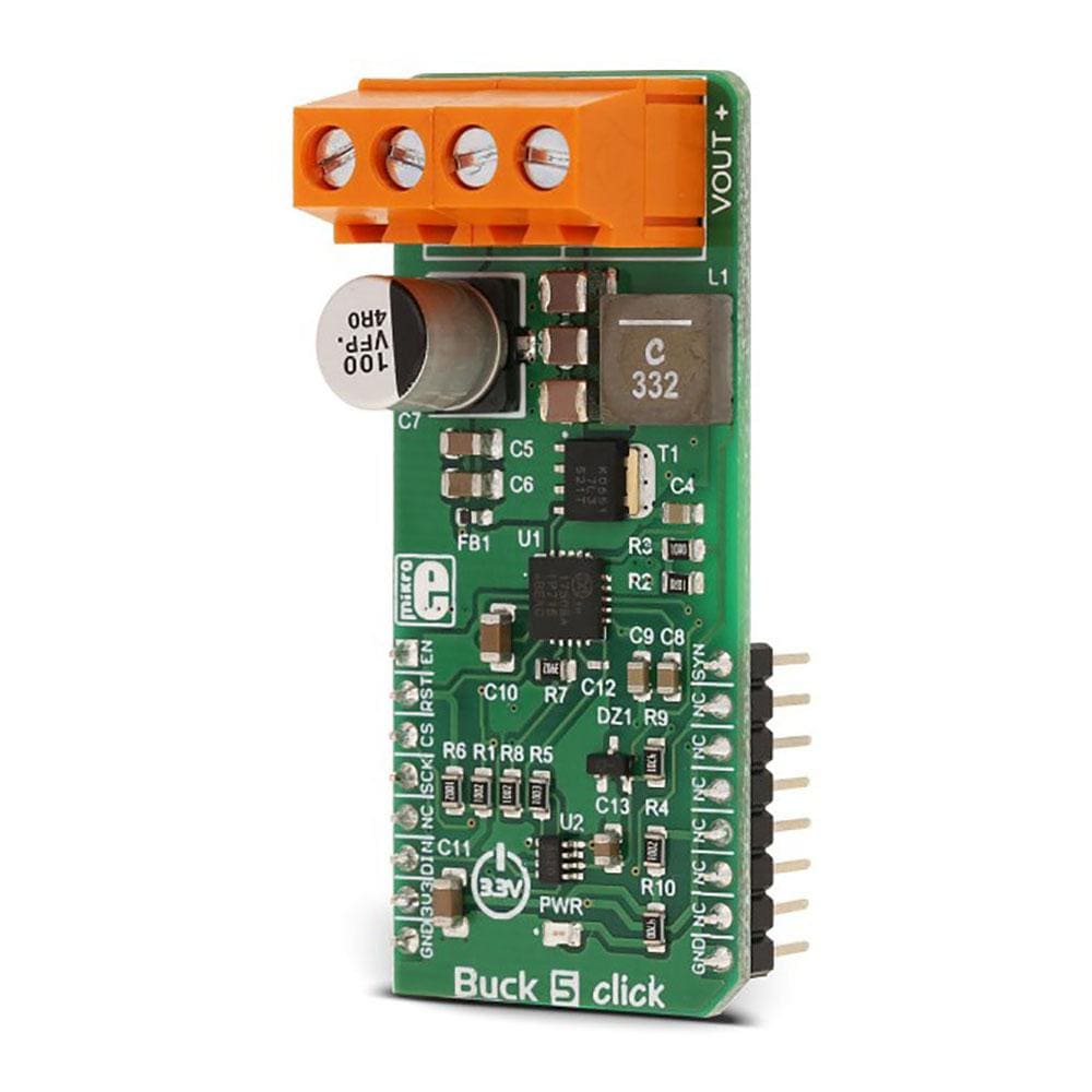
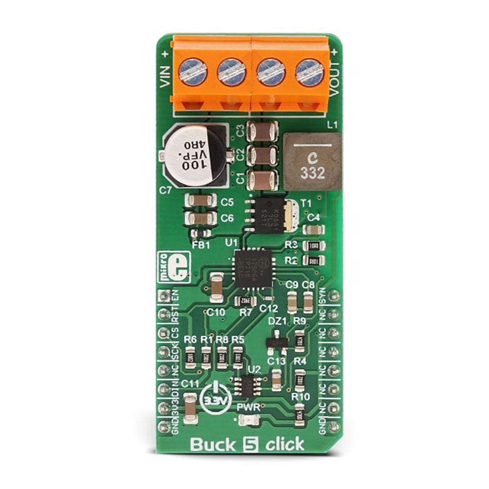
Buck 5 Click Board™
Buck 5 Click Board™
SKU: MIKROE-3100
Couldn't load pickup availability

Overview
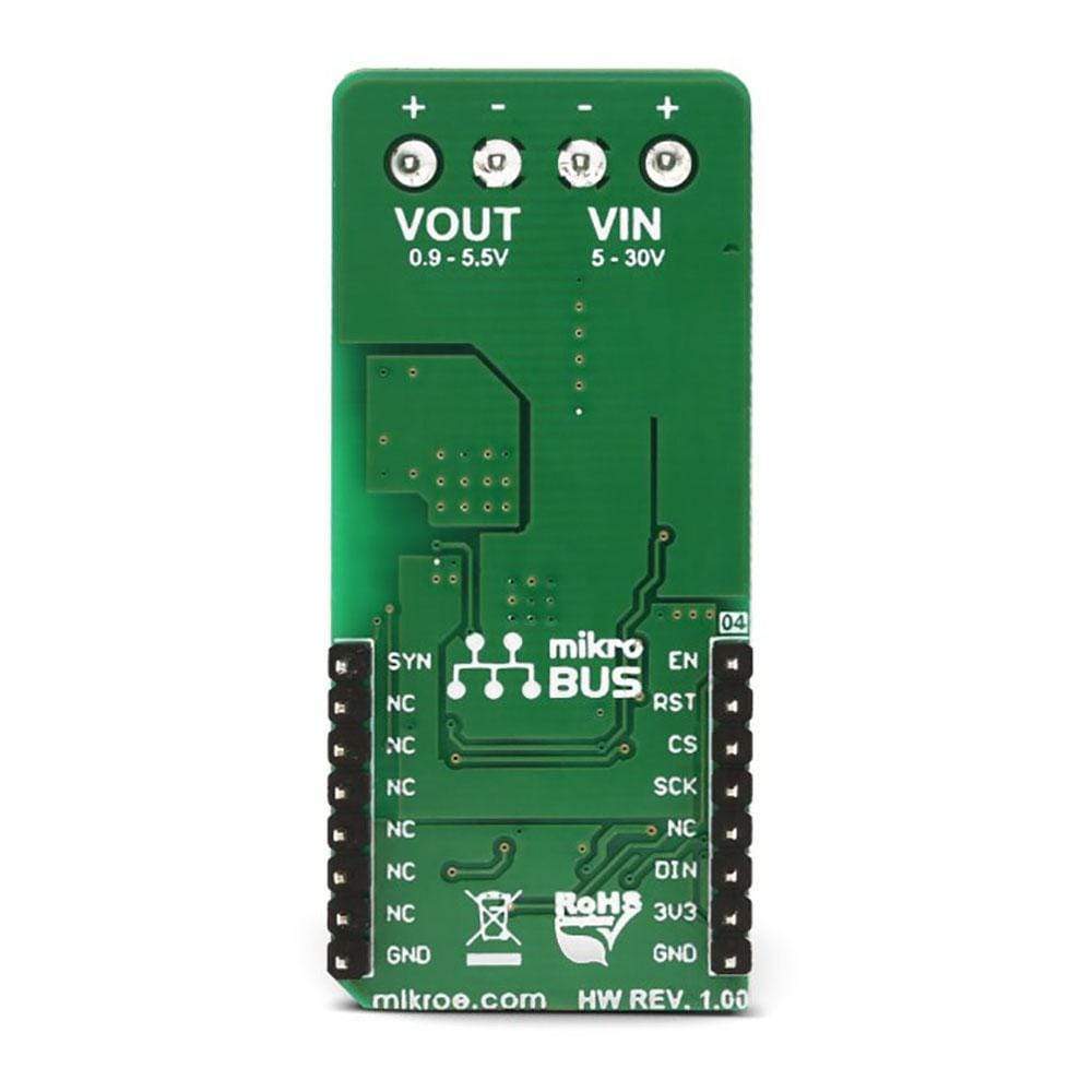
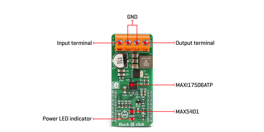
The Buck 5 Click Board™ is a high-efficiency buck (step-down) DC/DC converter, which can provide digitally adjusted step-down voltage on its output while delivering a considerable amount of current. Buck 5 Click Board™ accepts a wide voltage range on its input - from 5V to 30V. The output voltage may be adjusted via the SPI interface, in the range from 0.9V to approximately 5.5V. This Click Board™ utilises the MAX17506, an integrated high efficiency, synchronous step-down DC/DC converter with internal feedback compensation, from Maxim Integrated. In addition, the MAX5401 digital potentiometer with SPI Interface is used on the feedback loop allowing digital control of the output voltage.
Downloads
The Buck 5 Click Board™ is very useful for the development of applications that require programmed reduction of a wide input voltage range, so it can be used to power low voltage digital ICs. Features, such as the low dissipation due to high efficiency, three different operating modes, over-current, undervoltage and thermal protection, output voltage monitoring pin, make this Click Board™ very reliable power source for a range of applications, such as the distributed power supply regulation, wall transformer regulation, single board systems, general points of load, and similar applications.
How Does The Buck 5 Click Board™ Work?
Buck 5 Click Board™ is equipped with the MAX17506, a high efficiency, synchronous step-down DC/DC converter with internal compensation, from Maxim Integrated. This is an advanced step-down converter IC with an integrated high-side MOSFET, which requires a minimum number of external components, thanks to the internal feedback loop compensation. It utilizes a peak-current-mode control architecture. While the high side MOSFET is open and the current through the inductor ramps up, an over-current event will cause the MOSFET to close, preventing this current to become dangerously high. If there is a short circuit condition on the output, the device will reattempt to start after a timeout period, and if the condition is still present at the output, it will be turned off for another timeout period.
To allow adjustment of the output voltage via the SPI interface, the MAX5401, a 256-tap digital potentiometer with a SPI Interface made by Maxim, is used on the feedback loop. It is used in the place of the fixed voltage divider found on the reference design of the MAX17506, regulating the output voltage to a programmed value that way. As a result, by sending a digital value through the SPI interface to the MAX5401, it is possible to control the output voltage level in the range from 0.9V to 5.5V.
While operating normally (PWM mode), the high and the low side MOSFETs are switched synchronously with the signal from the internal PWM generator, causing the current through the inductor to ramp up and down, regulating the output voltage that way. The lower pulse width (duty cycle) of the PWM signal, results in a lower voltage at the output. The low side MOSFET is placed outside of the IC, allowing less dissipation on the DC/DC converter IC.
Besides the PWM mode, the device is also capable of operating in the PFM mode (Pulse Frequency Modulation). This mode allows even higher efficiency for light loads, as the low side MOSFET is completely unused. The high side MOSFET charges the inductor, letting the load drain it. During this period, the IC is in the hibernation state. This mode results in slightly more ripple at the output, with the added benefit of high efficiency for light loads. It is perfectly suited to power devices which are in the low-power consumption mode (Sleep, Standby…)
The DCM mode is the compromise mode between PWM and PFM modes. The low side MOSFET is still not used for light loads, but the PWM pulses are not skipped, and the IC constantly drives the high side MOSFET. This mode produces ripple at the output but it is slightly less efficient than the PFM mode for light loads.
Different modes are selected by the MODE/SYNC pin. By default, the IC is set to work in DCM mode, with the pull-up resistor. The MODE/SYNC pin of the IC is routed to the mikroBUS PWM pin (labelled as SYN), allowing the MCU to control the mode. When this pin is set to a LOW logic level, the constant frequency PWM mode is set.
The same pin (MODE/SYNC) can be used to synchronize the switching frequency of the converter IC (fs), when needed. This frequency is determined by the 39K resistor to about 480 kHz. However, the frequency can be synchronized with an external source in the range from 1.1 x fs, to 1.4 x fs.
The #RESET pin of the IC is routed to the mikroBUS RST pin. This pin signalizes problems with the output voltage. The pin is driven to a LOW logic level, when the output voltage drops under 92% of the nominal value, or during the thermal shutdown. It is an open drain output and it is otherwise pulled to a HIGH logic level (when not asserted).
To enable the buck converter IC, a HIGH logic level needs to be present at the EN pin of the IC, routed to the mikroBUS AN pin (labelled as EN). This allows the MCU to effectively control the Power ON function of the Click Board™. When the IC is enabled, the LED indicator labelled as EN will indicate that the IC is activated, and the step-down conversion is in progress. Soft-start circuit prevents high inrush currents by introducing a ramp-up of the output voltage, from 0V up to the nominal value.
SPECIFICATIONS
| Type | Buck |
| Applications | A regulated power source for wide range of applications, such as the digital IC power supply, wall transformer regulation, single board systems, general points of load, and similar applications |
| On-board modules | MAX17506, a high efficiency, synchronous step-down DC-DC converter with internal compensation, from Maxim Integrated; MAX5401, a 256-tap digital potentiometer with SPI Interface, from Maxim |
| Key Features | low-power dissipation due to high efficiency, three different operating modes, over-current, undervoltage and thermal protection, output voltage monitoring pin, output voltage set by the industry standard SPI interface |
| Interface | SPI |
| Compatibility | mikroBUS |
| Click Board™ size | L (57.15 x 25.4 mm) |
| Input Voltage | 3.3V |
ONBOARD JUMPERS AND SETTINGS
| Label | Name | Default | Description |
|---|---|---|---|
| LD1 | PWR | - | Power LED indicator |
| TB1 | VIN | - | External power supply input connector |
| TB2 | VOUT | - | Regulated voltage output connector |
BUCK 5 Click Board™ ELECTRICAL SPECIFICATIONS
| Description | Min | Typ | Max | Unit |
|---|---|---|---|---|
| Output voltage | 0.9 | - | 5.5 | V |
| Input voltage | 5 | - | 30 | V |
| Output current | 0 | - | 5 | A |
This table shows how the pinout on Buck 5 Click Board™ corresponds to the pinout on the mikroBUS socket (the latter shown in the two middle columns).
| Notes | Pin | Pin | Notes | ||||
|---|---|---|---|---|---|---|---|
| Buck Enable | EN | 1 | AN | PWM | 16 | SYN | |
| Voltage Monitor OUT | RST | 2 | RST | INT | 15 | NC | |
| Chip Select | CS | 3 | CS | RX | 14 | NC | |
| SPI Clock | SCK | 4 | SCK | TX | 13 | NC | |
| NC | 5 | MISO | SCL | 12 | NC | ||
| SPI Data IN | DIN | 6 | MOSI | SDA | 11 | NC | |
| Power Supply | 3.3V | 7 | 3.3V | 5V | 10 | NC | |
| Ground | GND | 8 | GND | GND | 9 | GND | Ground |
| General Information | |
|---|---|
Part Number (SKU) |
MIKROE-3100
|
Manufacturer |
|
| Physical and Mechanical | |
Weight |
0.028 kg
|
| Other | |
EAN |
8606018713288
|
Frequently Asked Questions
Have a Question?
Be the first to ask a question about this.