
Mikroelektronika d.o.o.
PLL Click Board™
PLL Click Board™
SKU: MIKROE-2993
Couldn't load pickup availability


Overview
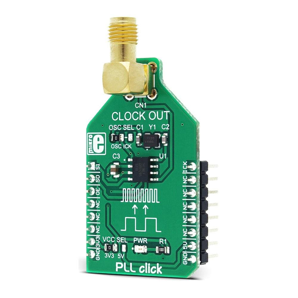
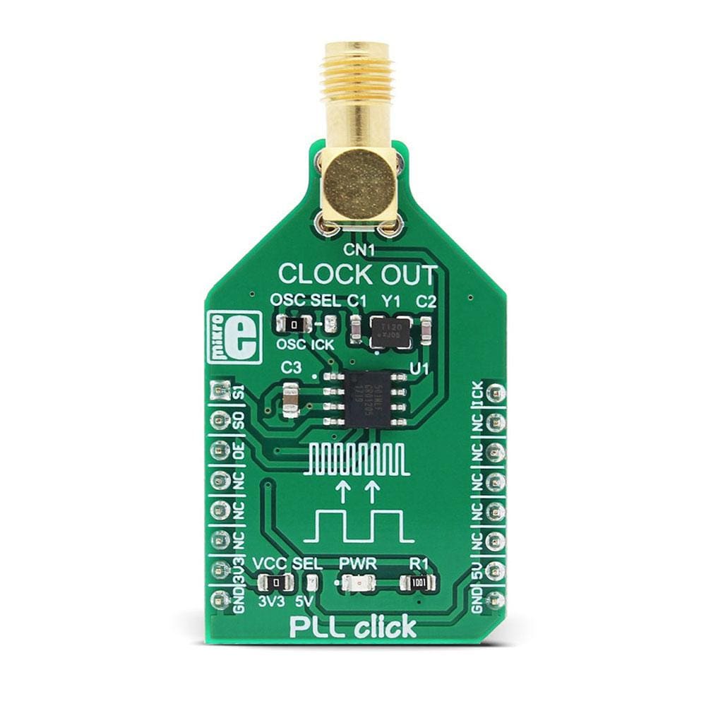
The PLL Click Board™ is a frequency multiplier that uses the Phase-Locked Loop (PLL) techniques to provide a high-frequency clock output from a cheap, standard fundamental mode crystal oscillator. In addition to this, PLL Click Board™ also offers a choice between nine different multiplication factors, programmed via states of the two input pins. The output range of the PLL Click Board™ goes up to 160MHz.
Downloads
The PLL Click Board™ is a frequency multiplier which uses the Phase-Locked Loop (PLL) techniques to provide a high-frequency clock output from a cheap, standard fundamental mode crystal oscillator. In addition to this, PLL click also offers a choice between nine different multiplication factors, programmed via states of the two input pins. The output range of the PLL click goes up to 160MHz.
Besides the fixed 12MHz crystal oscillator, the PLL Click Board™ can also use a PWM signal source brought from the PWM pin of the mikroBUS™, offering a possibility to continuously adjust the output frequency. Featuring a very precise PLL multiplication, very low output jitter of 25ps, tri-state output for board level testing, both onboard and external clock inputs, ability to change clock "on the fly", compatibility with all the 3.3V and 5V MCUs, and selectable multiplication factor, this Click board™ can be used for development and prototyping of various applications which can benefit from having an adjustable system clock generator, or for any general purpose application that demands cheap solution for the high-speed system clock.
How Does The PLL Click Board™ Work?
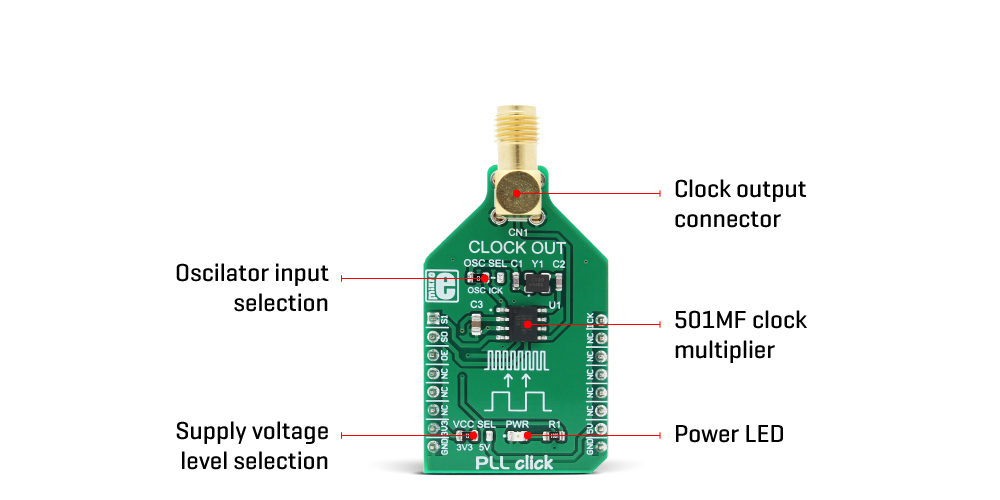
The PLL Click Board™ is equipped with the ICS501, a LOCO™ PLL clock multiplier, from Integrated Device Technology. This IC uses the Phase-Locked Loop to provide a high-frequency clock output, deriving input from a much cheaper, standard fundamental frequency crystal oscillator. Besides the onboard crystal oscillator fixed at 12MHz, it is possible to select the signal from the mikroBUS™ PWM pin as the clock input source.
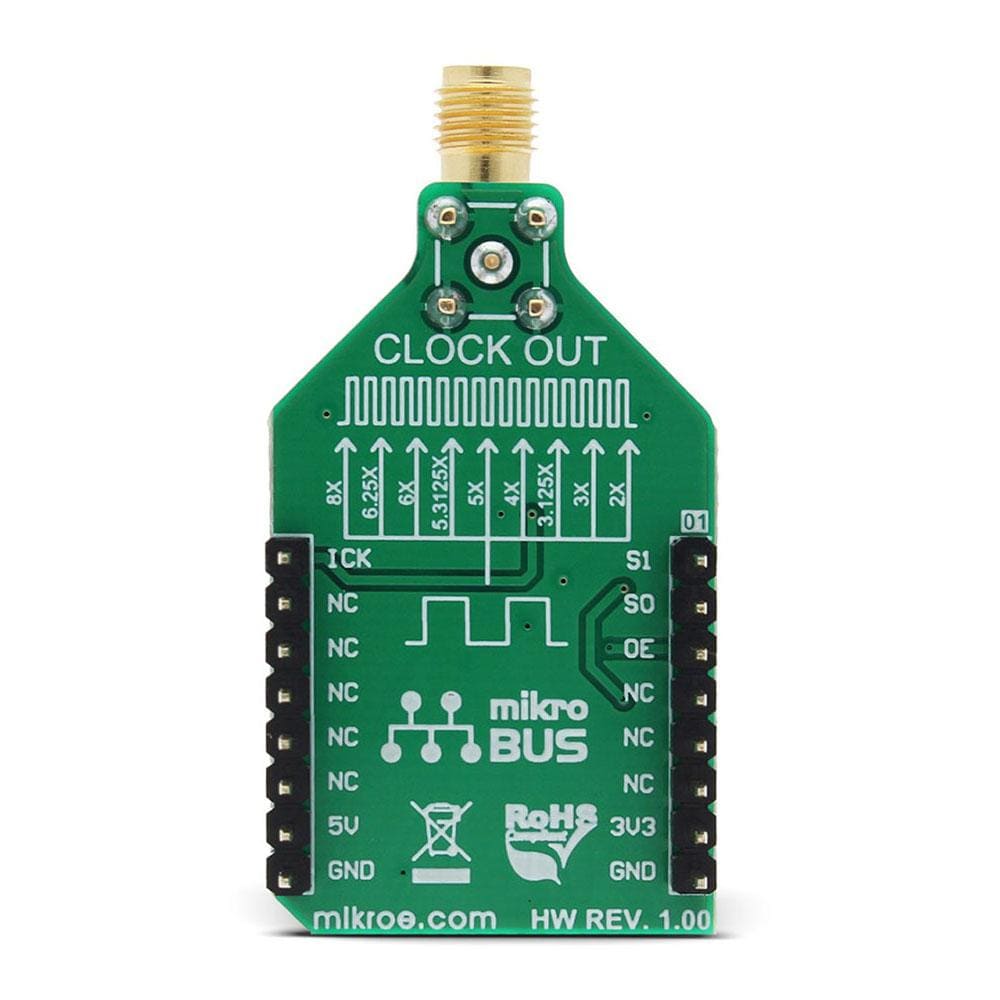
To select the desired multiplication factor, the states of the two input pins S0 and S1, routed to the mikroBUS™ pins RST and AN, respectively. These pins can be set to a HIGH logic state, LOW logic state, or can be disconnected (by tri-stating the MCU pins). The combination of these pins states will set the PLL click to a specific multiplier. To set the multiplication factor of the PLL click, please consult the multiplication selection table, below.
The Output Enable (OE) pin of the ICS501, is used to disable the output clock, by setting it to a LOW logic level. It will additionally set the clock output pin in high impedance (Hi-Z) mode, allowing complete disconnection and no influence on the rest of the circuit, which is useful for experimenting and prototyping purposes. This pin is internally pulled to a HIGH logic level. The OE pin is routed to the CS pin of the mikroBUS™.
The PLL Click Board™ is equipped with two onboard SMD jumpers. The SMD jumper labelled as the VCC SEL is used to select the operating voltage level, consequently limiting the amplitude of the clock output signal, in respect to the selected voltage. The other SMD jumper labelled as the OSC SEL is used to choose the clock input source between the onboard 12MHz crystal oscillator or the external clock signal. The output signal is routed through the onboard SMA connector, which provides a secure connection and good signal shielding.
The PLL Click Board™ comes with the library that contains functions for all the MikroElektronika compilers (mikroBASIC, mikroPASCAL, and mikroC). Although relatively easy to control it, the library offers comprehensive functions that make the code more readable and are easy to use. The included example application demonstrates the use of these functions and it can be used as a reference for custom projects.
SPECIFICATIONS
| Type | Clock generator |
| Applications | The PLL Click Board™ can be used for development and prototyping of various applications which can benefit from having an adjustable system clock generator, or for any general purpose application that demands cheap solution for the high-speed system clock. |
| On-board modules | ICS501, a LOCO™ PLL clock multiplier, from Integrated Device Technology |
| Key Features | Precise PLL multiplication, very low output jitter of 25ps, the tri-state output for board level testing, both onboard and external clock inputs, etc. |
| Interface | GPIO |
| Compatibility | mikroBUS |
| Click board size | M (42.9 x 25.4 mm) |
| Input Voltage | 3.3V or 5V |
PINOUT DIAGRAM
This table shows how the pinout of the PLL Click Board™ corresponds to the pinout on the mikroBUS™ socket (the latter shown in the two middle columns).
| Notes | Pin | Pin | Notes | ||||
|---|---|---|---|---|---|---|---|
| Multiplier adjustment pin 1 | S1 | 1 | AN | PWM | 16 | ICK | External clock source |
| Multiplier adjustment pin 0 | S0 | 2 | RST | INT | 15 | NC | |
| Output enable | OE | 3 | CS | RX | 14 | NC | |
| NC | 4 | SCK | TX | 13 | NC | ||
| NC | 5 | MISO | SCL | 12 | NC | ||
| NC | 6 | MOSI | SDA | 11 | NC | ||
| Power supply | +3.3V | 7 | 3.3V | 5V | 10 | +5V | Power supply |
| Ground | GND | 8 | GND | GND | 9 | GND | Ground |
PLL CLICK SPECIFICATIONS
| Description | Min | Typ | Max | Unit |
|---|---|---|---|---|
| Input frequency - crystal input | - | 12 | - | MHz |
| Input frequency - clock input | 2 | - | 50 | MHz |
| Absolute clock period jitter | -75 | - | 75 | ps |
ONBOARD SETTINGS AND INDICATORS
| Label | Name | Default | Description |
|---|---|---|---|
| LD1 | PWR | - | Power LED indicator |
| JP1 | VCC SEL | Left | Power supply voltage selection: left position 3V3, right position 5V |
| JP2 | OSC SEL | Left | Input clock signal source selection: left position onboard 12MHz crystal oscillator, right position external clock from PWM pin |
| General Information | |
|---|---|
Part Number (SKU) |
MIKROE-2993
|
Manufacturer |
|
| Physical and Mechanical | |
Weight |
0.021 kg
|
| Other | |
EAN |
8606018712830
|
Frequently Asked Questions
Have a Question?
Be the first to ask a question about this.