


Mikroelektronika d.o.o.
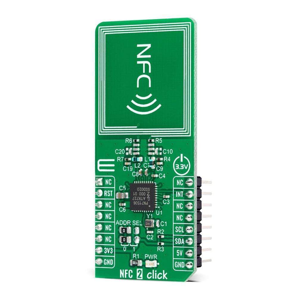
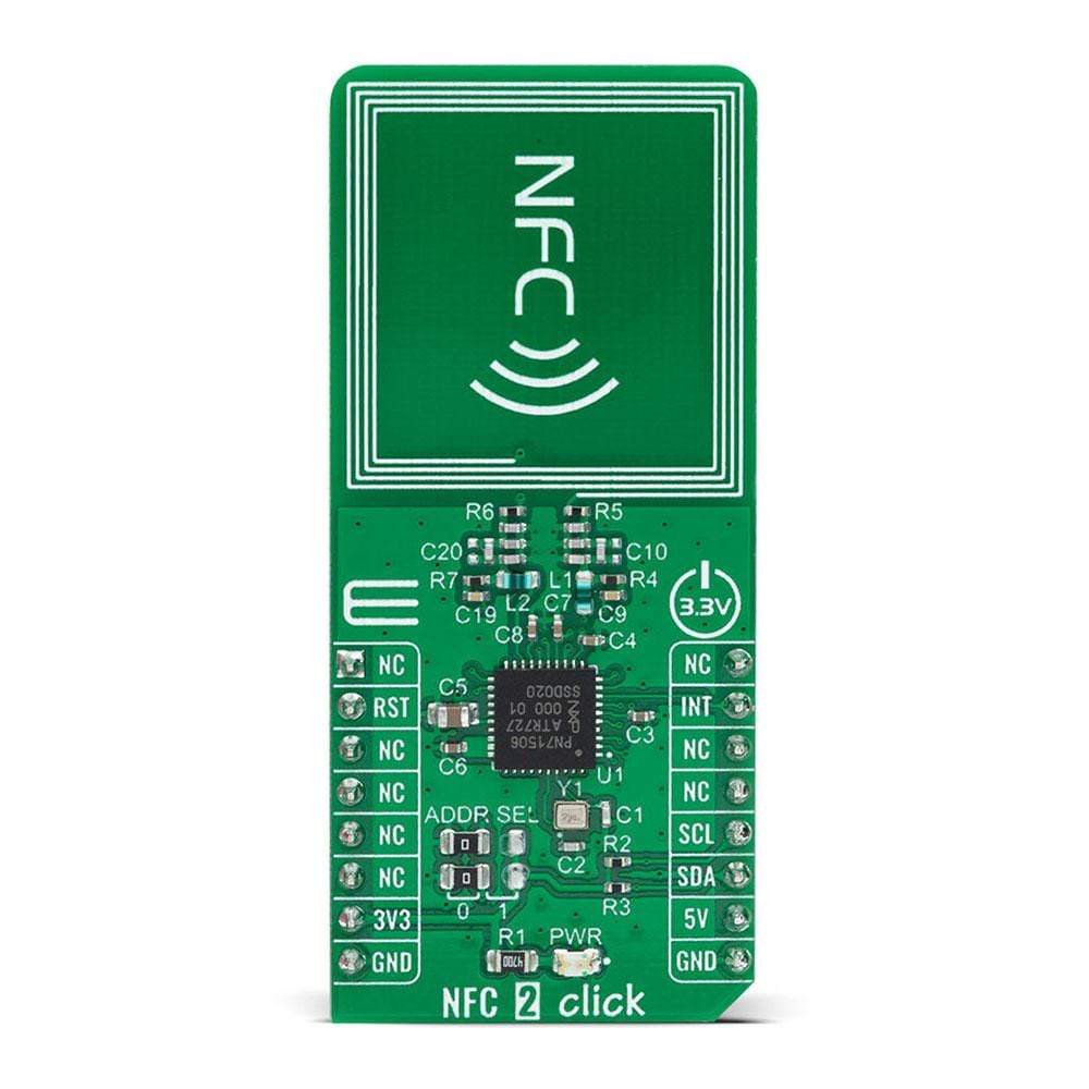
NFC 2 Click Board™
NFC 2 Click Board™
SKU: MIKROE-4309
Couldn't load pickup availability


Overview
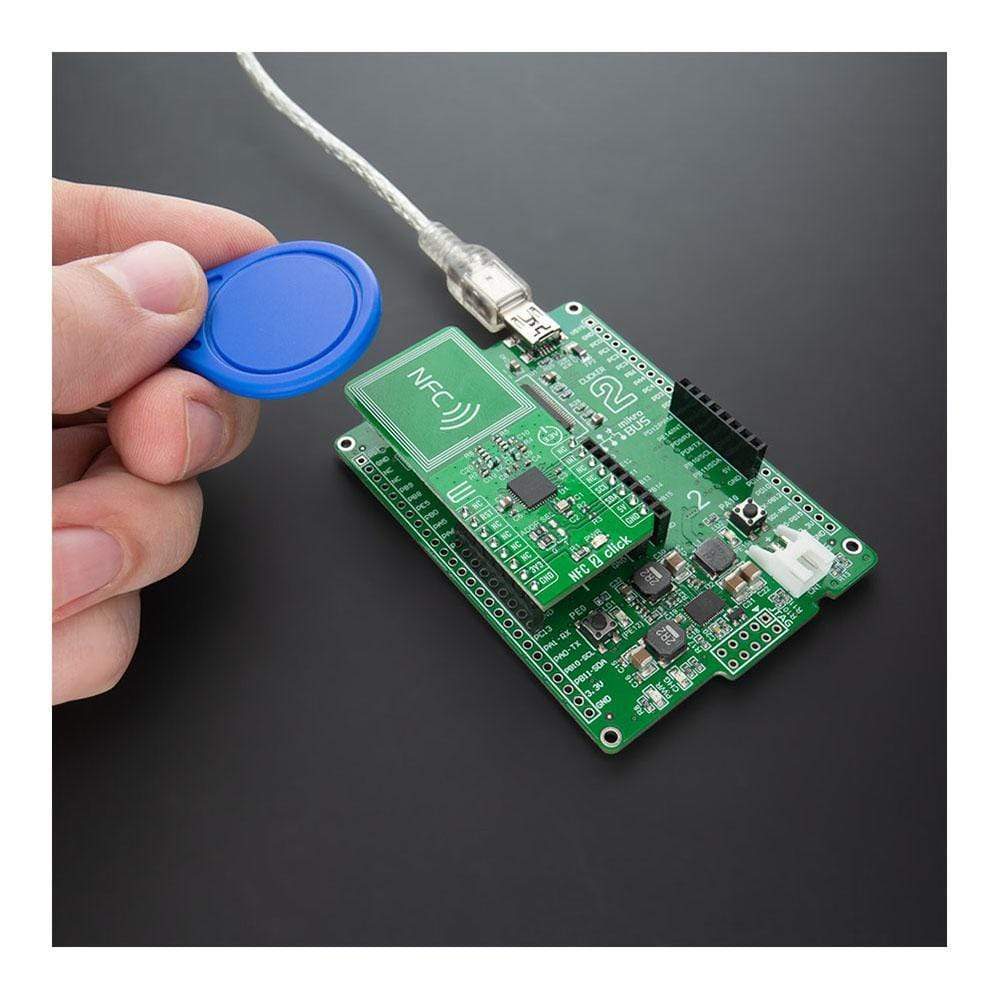
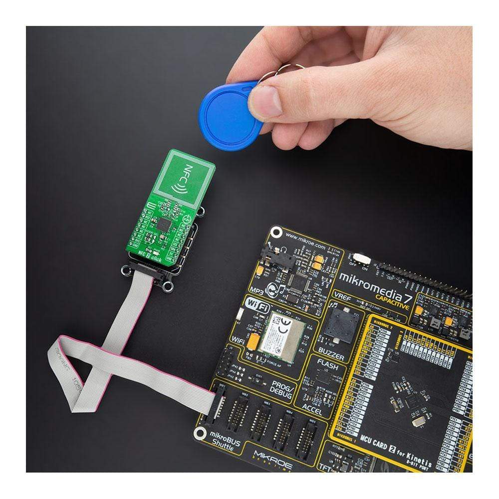
The NFC 2 Click Board™ is a compact add-on board that contains a highly integrated NFC transceiver for contactless communication. This board features the PN7150, the best plug&play high-performance full NFC solution with integrated firmware and NCI interface designed for contactless communication at 13.56 MHz from NXP USA Inc. This I2C configurable transceiver utilizes an outstanding modulation and demodulation concept completely integrated for different kinds of contactless communication methods and protocols. It can operate both in Reader Mode and in Card Mode. This Click Board™ is the ideal solution for rapidly integrating NFC technology in any application.
The NFC 2 Click Board™ is supported by a mikroSDK compliant library, which includes functions that simplify software development. This Click Board™ comes as a fully tested product, ready to be used on a system equipped with the mikroBUS™ socket.
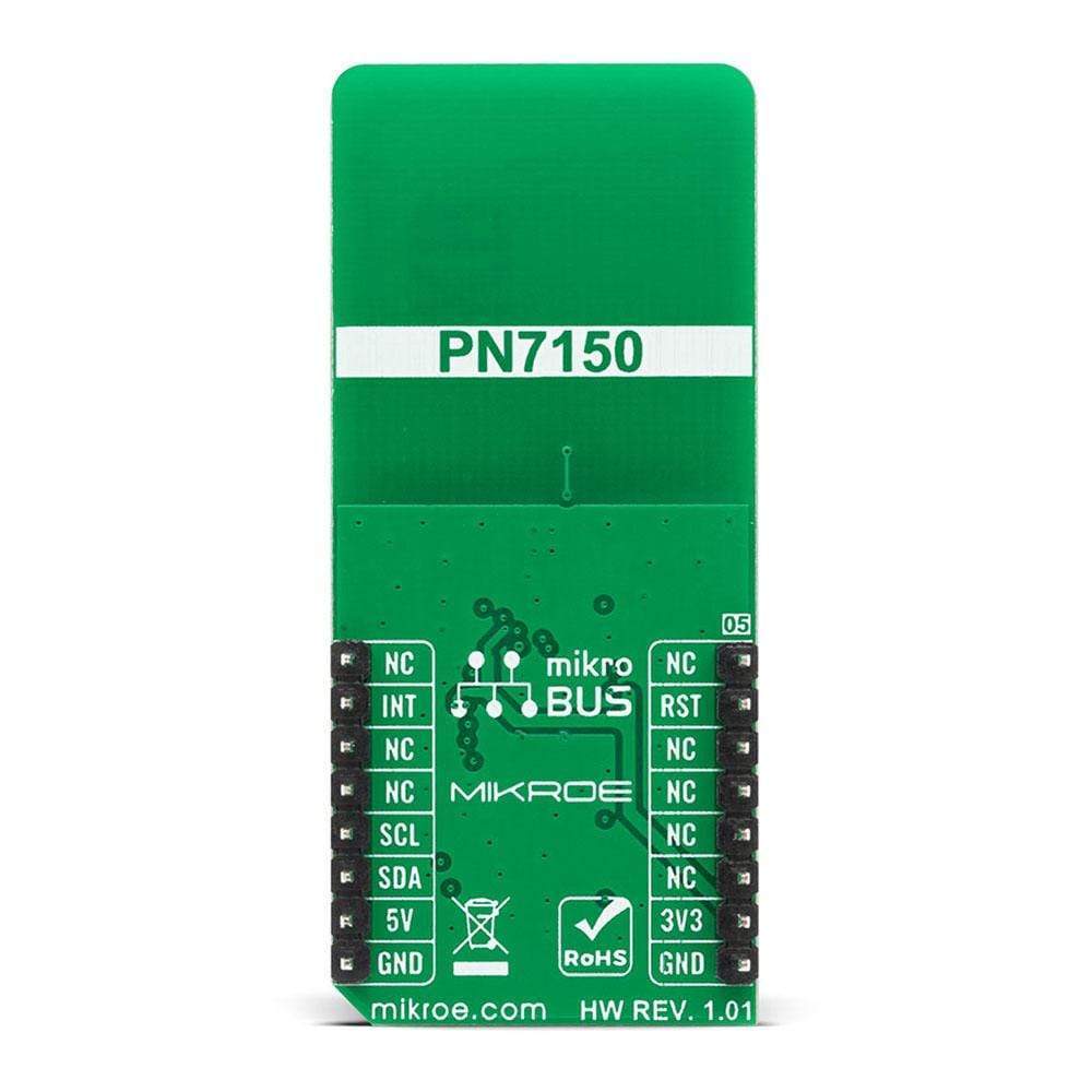
NOTE: Besides the Click board form factor, Mikroe offers a Dongle version also based on NXP’s PN7150 transceiver.
Downloads
How Does The NFC 2 Click Board™ Work?
The NFC 2 Click Board™ is based on the PN7150, high-performance full NFC solution with integrated firmware and I2C interface designed for contactless communication at 13.56 MHz from NXP USA Inc. This board has full compliance with NFC Forum specification that means that you will be able to use the full potential of NFC. It is the ideal solution for rapidly integrating NFC technology in any application, especially those running O/S environments like Linux and Android, reducing size and cost thanks to embedded NFC firmware providing all NFC protocols as a pre-integrated feature and ultra-low power consumption.
The PN7150 embeds a microcontroller core ARM Cortex-M0 loaded with the integrated firmware and provides an easy integration and validation cycle as all the NFC real-time constraints, protocols, and device discovery are being taken care of internally. The host can configure the PN7150 to notify for a card or peer detection and start communicating with them. The core microcontroller chip of the PN7150 can run without any external clock (based on an internal oscillator). However, the 13.56MHz RF field carrier accuracy requirements are not compatible with the use of an internal oscillator. That's why the PN7150 has an external crystal oscillator connected to its XTAL pins.
It also has four power states: Monitor, Hard Power Down (HPD), Standby, and Active. At the application level, the PN7150 will continuously switch between different power states to optimize the current consumption. The PN7150 is designed to allow the host controller to have full control over its operation, thus of the power consumption of the PN7150 based NFC solution and the possibility to restrict parts of the PN7150 functionality. More information about these modes user can find in the attached datasheet.
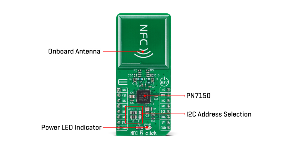
The NFC 2 Click Board™ communicates with MCU using the standard I2C 2-Wire interface with a clock frequency up to 100kHz in the Standard, up to 400kHz in the Fast, and up to 3.4MHz in the High-Speed Mode. The PN7150 also allows the choice of the least significant bit (LSB) of its I2C slave address by positioning SMD jumpers labelled as ADDR SEL to an appropriate position marked as 0 and 1. To enable and ensure data flow control between PN7150 and host controller, additionally, a dedicated interrupt line labelled as INT is provided that Active state is programmable. It also contains Reset function, and the RF antenna which is used to communicate over RF with a Tag (Card) and a Reader/Writer or a Peer device.
The NFC 2 Click Board™ is designed to be operated only with a 3.3V logic voltage level, while 5V is used as transmitter input supply voltage of PN7150. A proper logic voltage level conversion should be performed before the Click board™ is used with MCUs with different logic levels. However, the Click board™ comes equipped with a library that contains easy to use functions and an example code which can be used, as a reference, for further development.
SPECIFICATIONS
| Type | RFID/NFC |
| Applications | Can be used for rapidly integrating NFC technology in any application. |
| On-board modules | The NFC 2 Click Board™ is based on the PN7150, high-performance full NFC solution with integrated firmware and I2C interface designed for contactless communication at 13.56 MHz from NXP USA Inc. |
| Key Features | Ultralow power consumption, automatic wake-up via RF field, integrated non-volatile memory to store data and executable code for customization, various RF protocols supported, includes ARM Cortex-M0 microcontroller core, and more. |
| Interface | I2C |
| Compatibility | mikroBUS |
| Click board size | L (57.15 x 25.4 mm) |
| Input Voltage | 3.3V or 5V |
PINOUT DIAGRAM
This table shows how the pinout of the NFC 2 Click Board™ corresponds to the pinout on the mikroBUS™ socket (the latter shown in the two middle columns).
| Notes | Pin | Pin | Notes | ||||
|---|---|---|---|---|---|---|---|
| NC | 1 | AN | PWM | 16 | NC | ||
| Reset | RST | 2 | RST | INT | 15 | INT | Interrupt |
| NC | 3 | CS | RX | 14 | NC | ||
| NC | 4 | SCK | TX | 13 | NC | ||
| NC | 5 | MISO | SCL | 12 | SCL | I2C Clock | |
| NC | 6 | MOSI | SDA | 11 | SDA | I2C Data | |
| Power Supply | 3.3V | 7 | 3.3V | 5V | 10 | 5V | Power Supply |
| Ground | GND | 8 | GND | GND | 9 | GND | Ground |
ONBOARD SETTINGS AND INDICATORS
| Label | Name | Default | Description |
|---|---|---|---|
| LD1 | PWR | - | Power LED Indicator |
| JP1-JP2 | ADDR SEL | Left | I2C Address Selection: Left position 0, Right position 1 |
NFC 2 CLICK ELECTRICAL SPECIFICATIONS
| Description | Min | Typ | Max | Unit |
|---|---|---|---|---|
| Supply Voltage | -0.3 | 3.3 | 4.35 | V |
| Operating Frequency | - | 13.56 | 52 | MHz |
| Maximum RF Driver Current | - | - | 180 | mA |
| Maximum Output Power | - | - | 0.85 | W |
| Operating Temperature Range | -30 | +25 | +85 | °C |
| General Information | |
|---|---|
Part Number (SKU) |
MIKROE-4309
|
Manufacturer |
|
| Physical and Mechanical | |
Weight |
0.018 kg
|
| Other | |
EAN |
8606027381294
|
Frequently Asked Questions
Have a Question?
Be the first to ask a question about this.