


Mikroelektronika d.o.o.
Tableau de clic Flash 8
Tableau de clic Flash 8
SKU: MIKROE-5293
Impossible de charger la disponibilité du service de retrait


Key Features
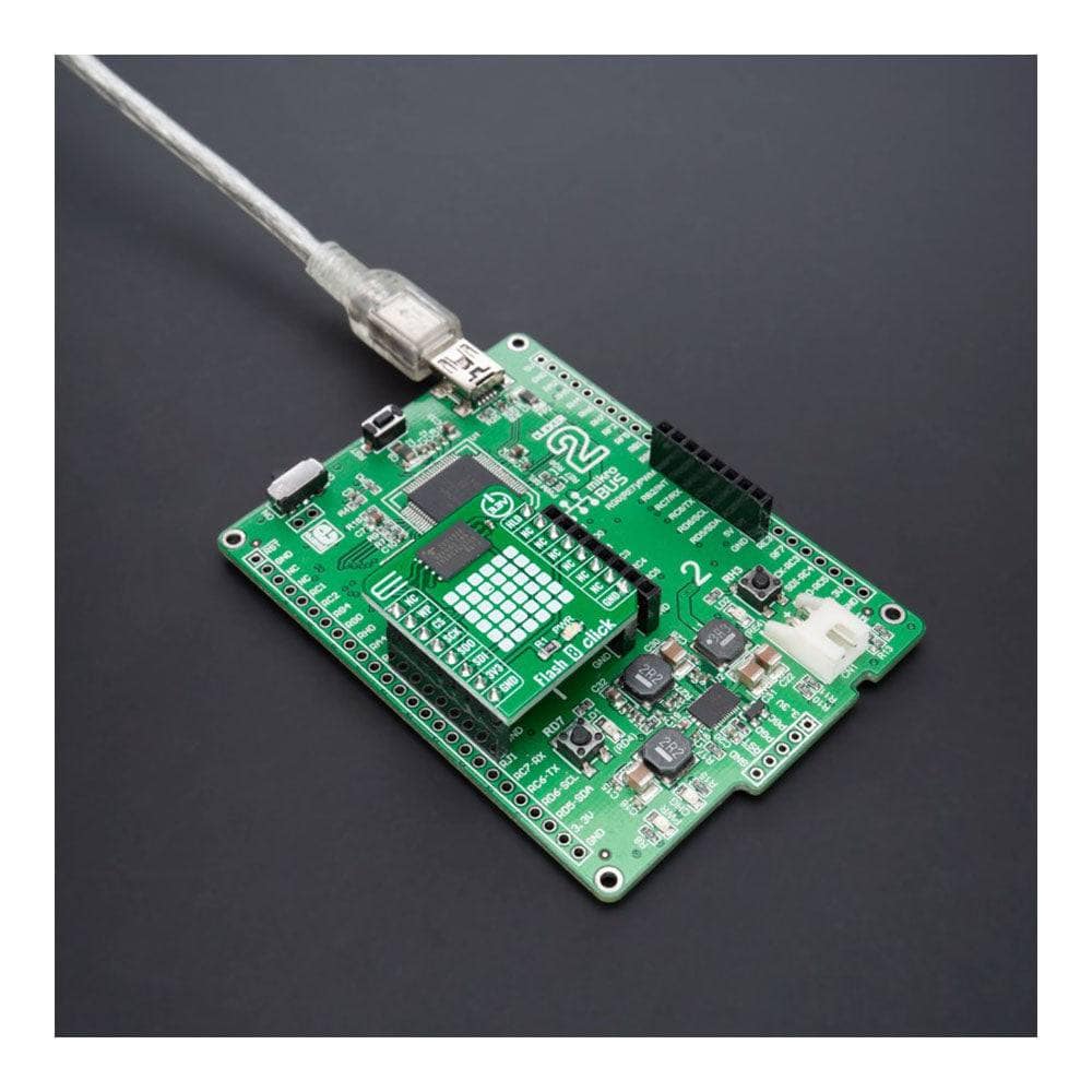
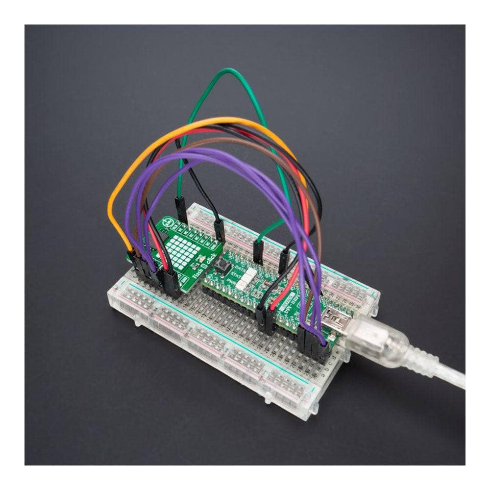
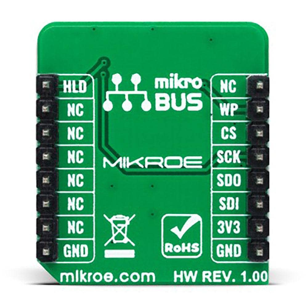
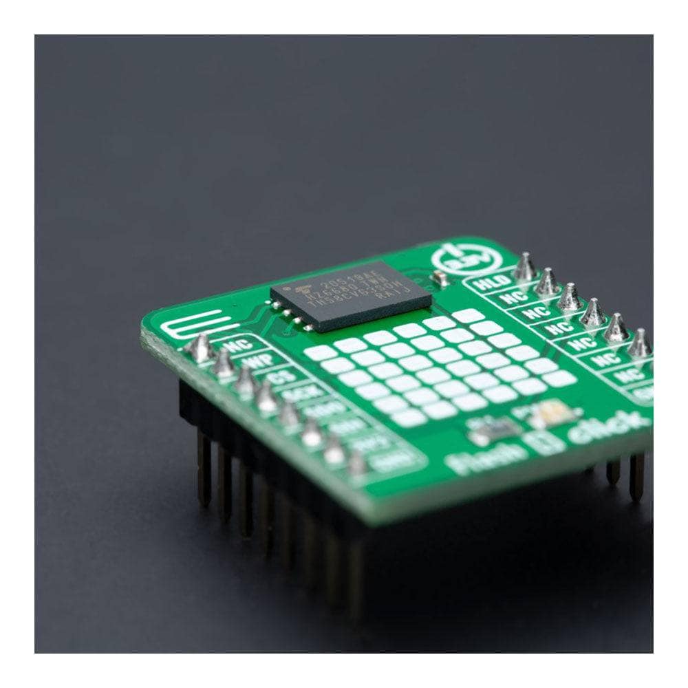
Overview
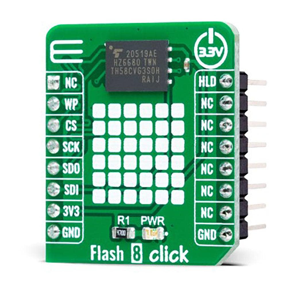
The Flash 8 Click Board™ is a compact add-on board representing a highly reliable memory solution. This board features the GD5F2GQ5UEYIGR, a 2Gb high-density non-volatile memory storage solution for embedded systems from GigaDevice Semiconductor. It is based on an industry-standard NAND Flash memory core, representing an attractive alternative to SPI-NOR and standard parallel NAND Flash with advanced features. The GD5F2GQ5UEYIGR also has advanced security features (8K-Byte OTP region), software/hardware write protection, can withstand many write cycles (minimum 100k), and has a data retention period greater than ten years. This Click board™ is suitable for storage and data transfer in consumer devices and industrial applications.
The Flash 8 Click Board™ is supported by a mikroSDK compliant library, which includes functions that simplify software development. This Click board™ comes as a thoroughly tested product, ready to be used on a system equipped with the mikroBUS™ socket.
Downloads
La carte Flash 8 Click Board™ est une carte complémentaire compacte représentant une solution de mémoire extrêmement fiable. Cette carte comprend le GD5F2GQ5UEYIGR , une solution de stockage de mémoire non volatile haute densité de 2 Go pour les systèmes embarqués de GigaDevice Semiconductor. Elle est basée sur un cœur de mémoire Flash NAND standard de l'industrie, représentant une alternative intéressante au SPI-NOR et au Flash NAND parallèle standard avec des fonctionnalités avancées. Le GD5F2GQ5UEYIGR dispose également de fonctionnalités de sécurité avancées (région OTP de 8 Ko), d'une protection en écriture logicielle/matérielle, peut supporter de nombreux cycles d'écriture (minimum 100 000) et dispose d'une période de conservation des données supérieure à dix ans. Cette carte Click™ convient au stockage et au transfert de données dans les appareils grand public et les applications industrielles.
La carte Flash 8 Click Board™ est supportée par une bibliothèque compatible mikroSDK, qui comprend des fonctions qui simplifient le développement logiciel. Cette carte Click Board™ est un produit entièrement testé, prêt à être utilisé sur un système équipé du socket mikroBUS™.
| General Information | |
|---|---|
Part Number (SKU) |
MIKROE-5293
|
Manufacturer |
|
| Physical and Mechanical | |
Weight |
0.02 kg
|
| Other | |
EAN |
8606027387890
|
Frequently Asked Questions
Have a Question?
Be the first to ask a question about this.