


Mikroelektronika d.o.o.
Tableau de clic Clock Gen
Tableau de clic Clock Gen
SKU: MIKROE-4113
Impossible de charger la disponibilité du service de retrait


Overview
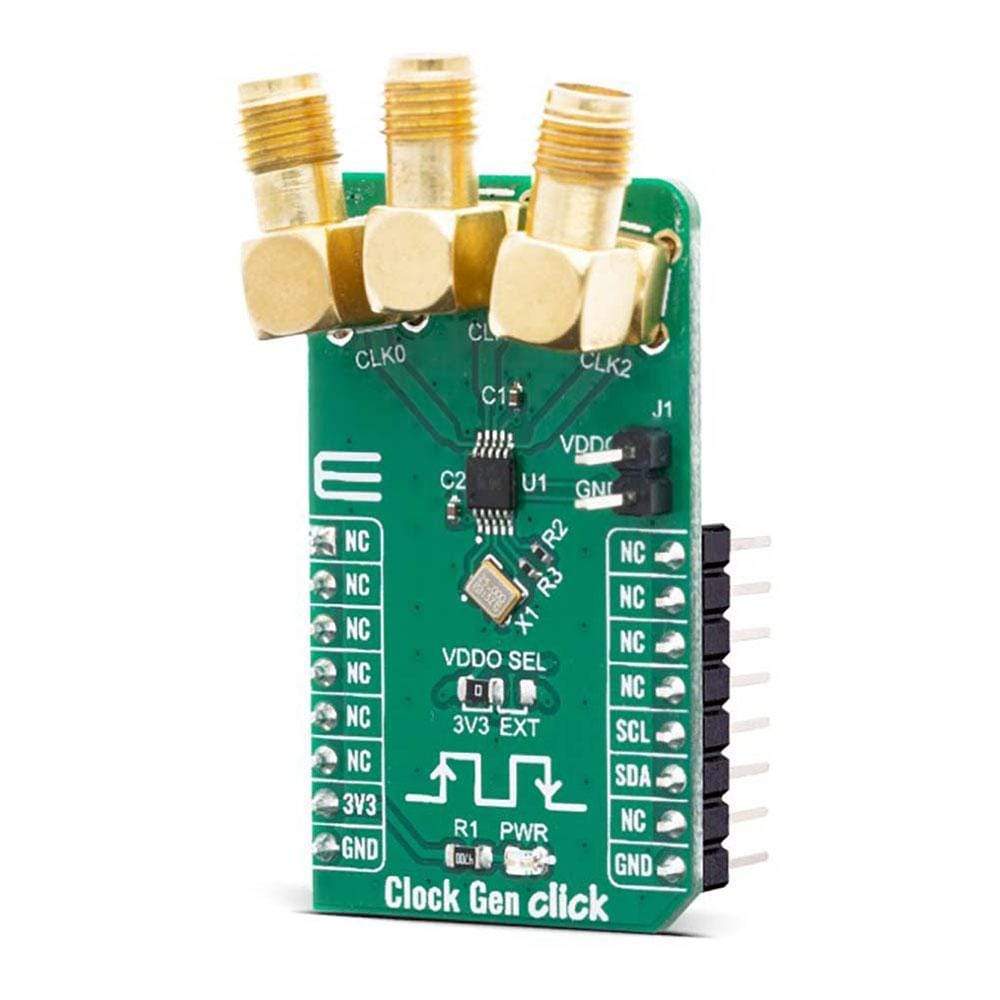
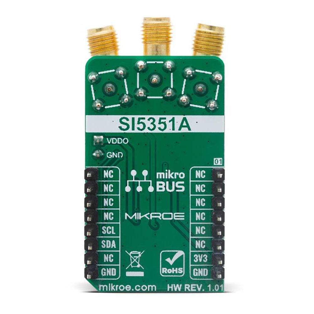
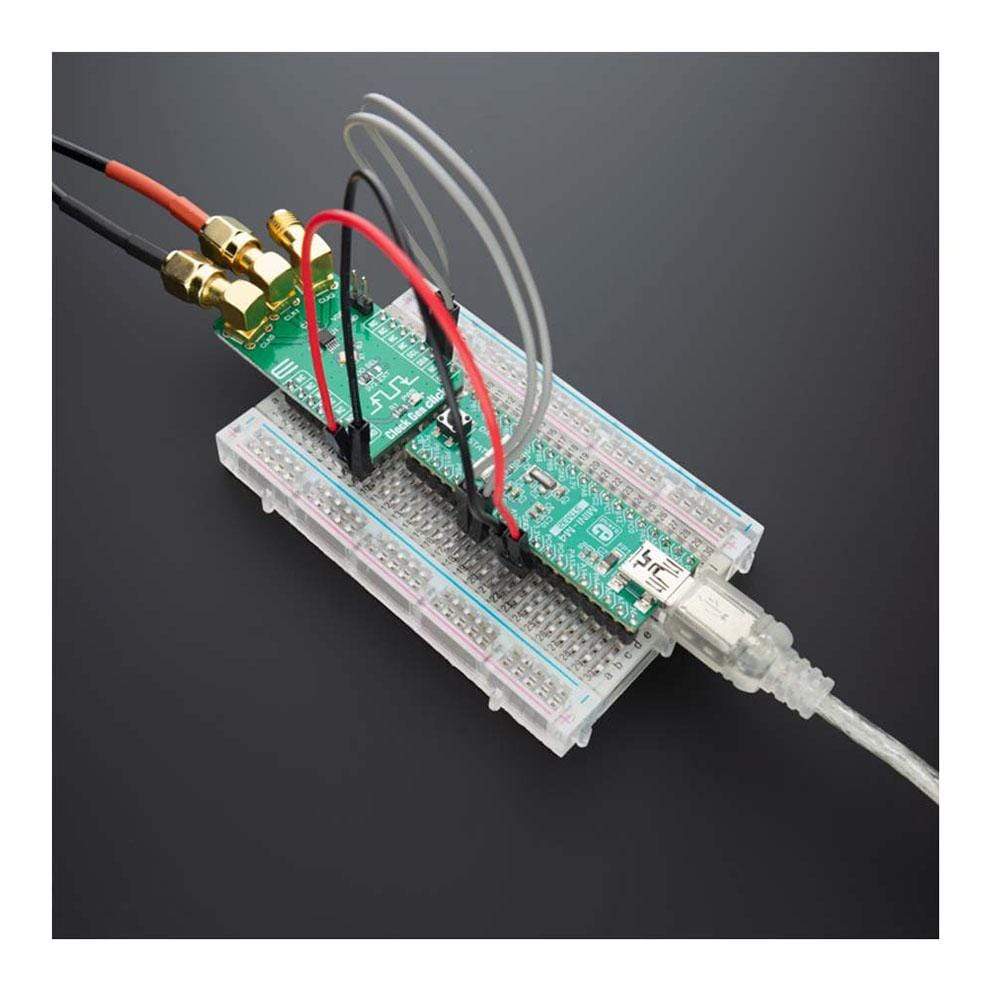
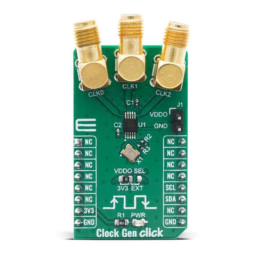
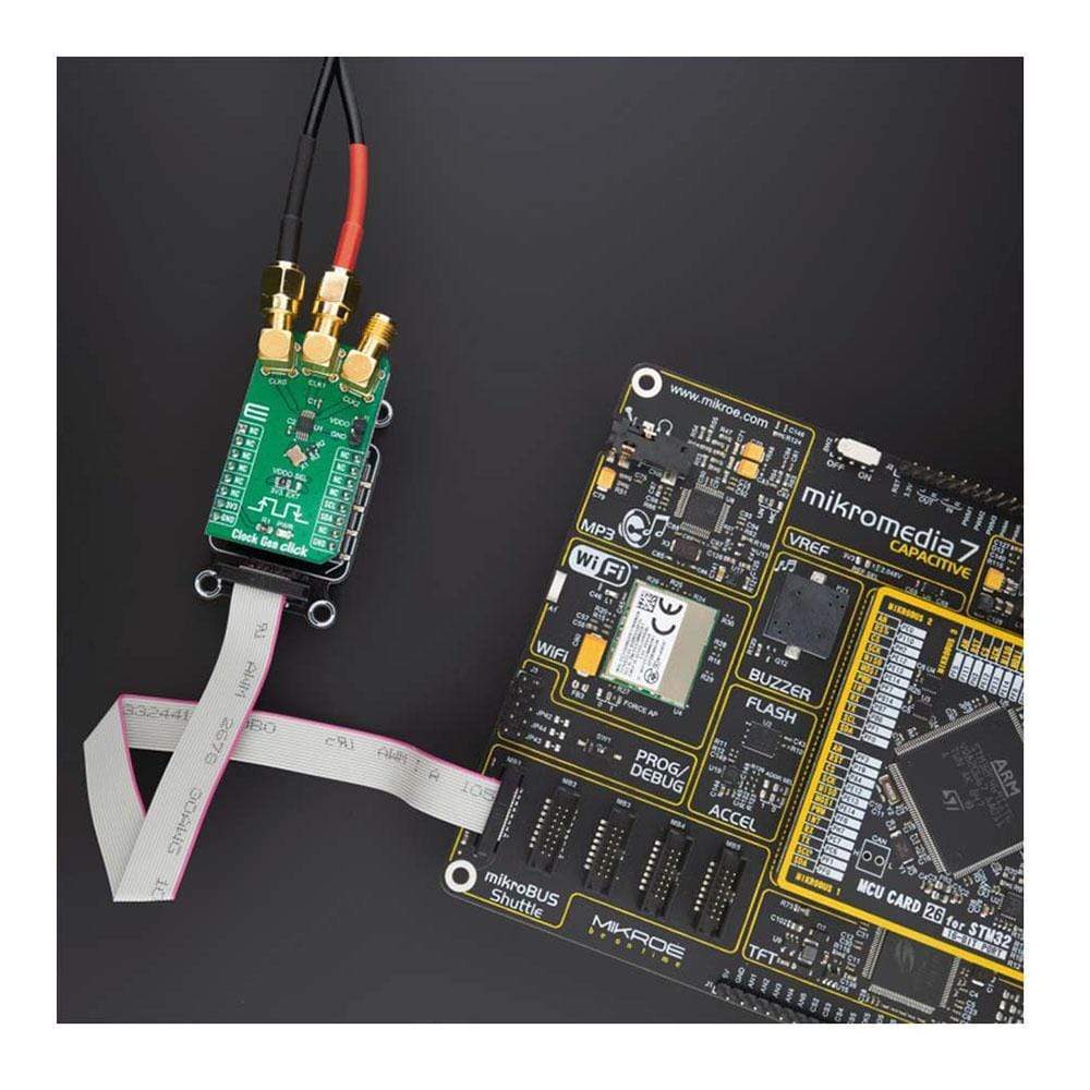
The Clock Gen Click Board™ offers an ideal replacement for crystals, crystal oscillators, VCXOs, phase-locked loops (PLLs), and fanout buffers in cost-sensitive applications. This Click Board™ features the Si5351A from Silicon Labs, an I2C configurable clock generator based on a PLL + high-resolution MultiSynth fractional divider architecture which can generate any frequency up to 200 MHz on each of its outputs with 0 ppm error.
The Si5351A is capable of generating synchronous or free-running non-integer related clock frequencies at each of its outputs (CLK0, CLK1, and CLK2), enabling one device to synthesize clocks for multiple clock domains in a design. It eliminates the need for higher cost, custom pullable crystals while providing reliable operation over a wide tuning range. The Si5351C offers the same flexibility but synchronizes to an external reference clock.
Downloads
Le Clock Gen Click Board™ constitue un remplacement idéal pour les cristaux, les oscillateurs à cristal, les VCXO, les boucles à verrouillage de phase (PLL) et les tampons de sortance dans les applications sensibles aux coûts. Ce Click Board™ est doté du Si5351A de Silicon Labs, un générateur d'horloge configurable I2C basé sur une architecture PLL + diviseur fractionnaire MultiSynth haute résolution qui peut générer n'importe quelle fréquence jusqu'à 200 MHz sur chacune de ses sorties avec une erreur de 0 ppm.
Le Si5351A est capable de générer des fréquences d'horloge non entières synchrones ou libres à chacune de ses sorties (CLK0, CLK1 et CLK2), ce qui permet à un seul appareil de synthétiser des horloges pour plusieurs domaines d'horloge dans une conception. Il élimine le besoin de cristaux personnalisés plus coûteux tout en offrant un fonctionnement fiable sur une large plage de réglage. Le Si5351C offre la même flexibilité mais se synchronise sur une horloge de référence externe.
| General Information | |
|---|---|
Part Number (SKU) |
MIKROE-4113
|
Manufacturer |
|
| Physical and Mechanical | |
Weight |
0.021 kg
|
| Other | |
EAN |
8606018717439
|
Frequently Asked Questions
Have a Question?
Be the first to ask a question about this.