


Mikroelektronika d.o.o.
Carte I2C MUX 2 Click
Carte I2C MUX 2 Click
SKU: MIKROE-4094
Impossible de charger la disponibilité du service de retrait


Overview
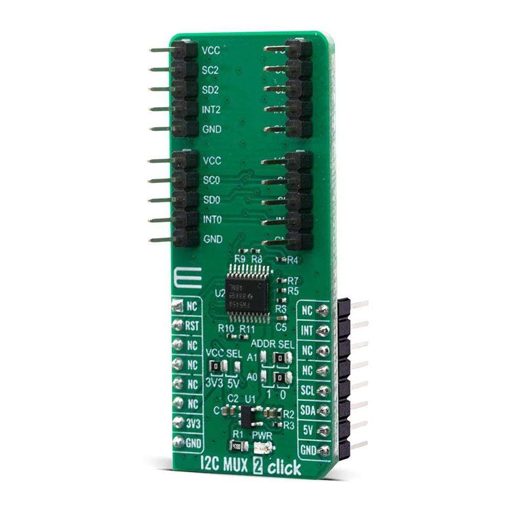
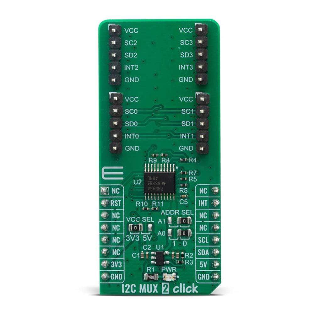
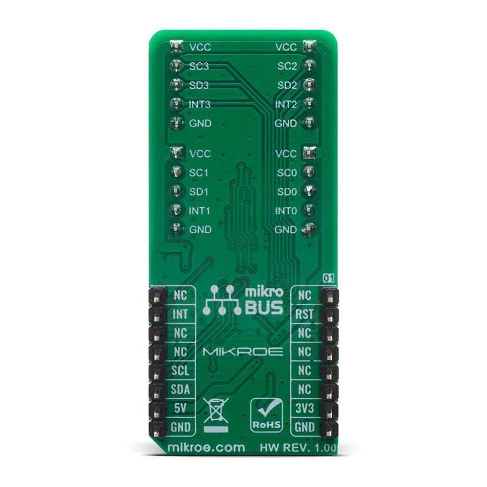
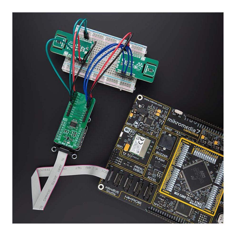
The I2C MUX 2 Click Board™ is a quad bidirectional translating I2C and SMBus switch with reset and interrupt functions, intended for applications with I2C slave address conflicts. It features a quad bidirectional translating switch controlled via the I2C bus, labelled as TCA9545A from Texas Instruments. Four interrupt inputs (INT3–INT0), one for each of the downstream pairs, are provided on the click board. One interrupt (INT) output acts as an AND of the four interrupt inputs. Click has two address jumpers, allowing up to four TCA9545A devices on the same bus. The I2C MUX 2 Click Board™ allows voltage translation between 1.8V, 2.5V, 3.3V, and 5V buses, and also supports hot insertion. The TCA9546A can work on a 0 - 400 kHz clock frequency range and is ideal for communication with numerous devices that share the identical slave address on the same bus.
The I2C MUX 2 Click Board™ is supported by a mikroSDK compliant library, which includes functions that simplify software development. This Click Board™ comes as a fully tested product, ready to be used on a system equipped with the mikroBUS™ socket.
Downloads
Le I2C MUX 2 Click Board™ est un commutateur I2C et SMBus de traduction bidirectionnel quadruple avec fonctions de réinitialisation et d'interruption, destiné aux applications avec conflits d'adresses esclaves I2C. Il est doté d'un commutateur de traduction bidirectionnel quadruple contrôlé via le bus I2C, étiqueté TCA9545A de Texas Instruments. Quatre entrées d'interruption (INT3–INT0), une pour chacune des paires en aval, sont fournies sur la carte Click. Une sortie d'interruption (INT) agit comme un ET des quatre entrées d'interruption. Click dispose de deux cavaliers d'adresse, permettant jusqu'à quatre périphériques TCA9545A sur le même bus. Le I2C MUX 2 Click Board™ permet la traduction de tension entre les bus 1,8 V, 2,5 V, 3,3 V et 5 V, et prend également en charge l'insertion à chaud. Le TCA9546A peut fonctionner sur une plage de fréquences d'horloge de 0 à 400 kHz et est idéal pour la communication avec de nombreux périphériques qui partagent la même adresse esclave sur le même bus.
La carte Click Board™ I2C MUX 2 est prise en charge par une bibliothèque compatible mikroSDK, qui comprend des fonctions qui simplifient le développement logiciel. Cette carte Click Board™ est un produit entièrement testé, prêt à être utilisé sur un système équipé du socket mikroBUS™.
| General Information | |
|---|---|
Part Number (SKU) |
MIKROE-4094
|
Manufacturer |
|
| Physical and Mechanical | |
Weight |
0.021 kg
|
| Other | |
EAN |
8606018717347
|
Frequently Asked Questions
Have a Question?
Be the first to ask a question about this.