


Mikroelektronika d.o.o.
Carte à clic LLC-I2C
Carte à clic LLC-I2C
SKU: MIKROE-3276
Impossible de charger la disponibilité du service de retrait


Key Features
Overview
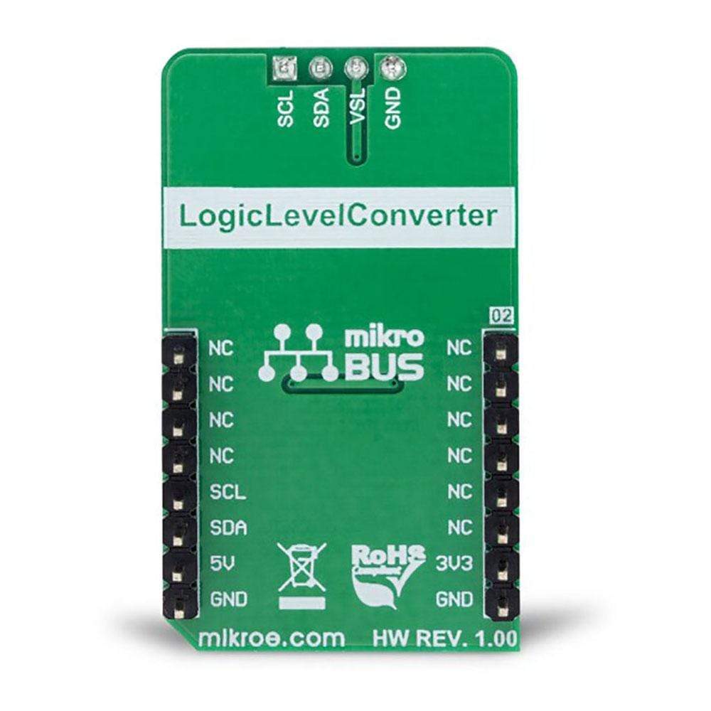
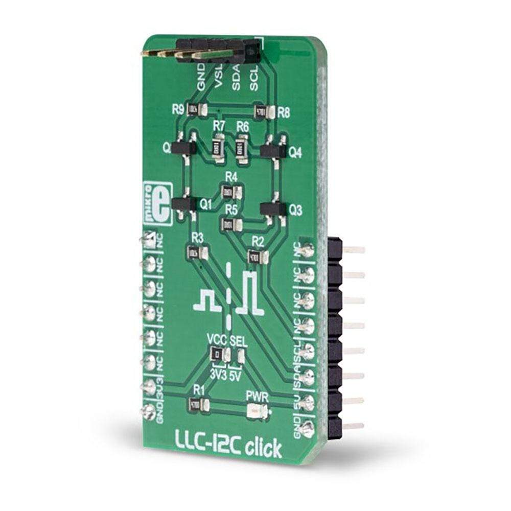
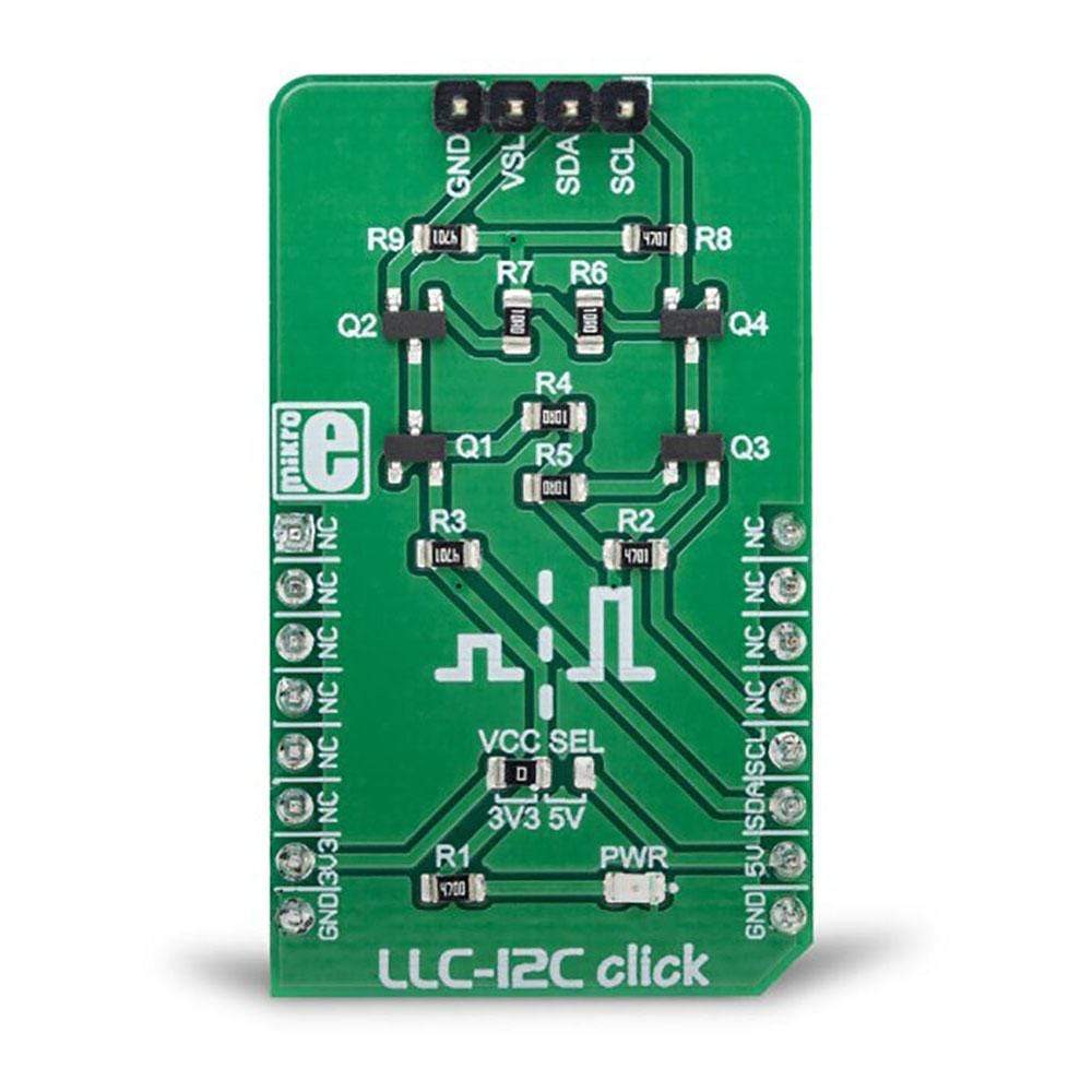
The LLC I2C Click Board™ can be utilized as the level converter for logic signals, which makes it a very useful Click Board™. The topology of this logic level conversion (LLC) circuit is perfectly suited for the bi-directional I2C communication. Although there are some specialised integrated circuits on the market, sometimes it is more convenient to have a simple solution made of just a few passive elements and four MOSFETs. Besides this, MOSFETs can withstand up to 20V across their terminals (12V VGS), and they support far greater currents than typical ICs, making them less likely to fail. The LLC circuitry, also known as the level translator or level shifter, can be used in virtually any application that utilizes the I2C communication protocol and needs matching between the logic voltage levels
Downloads
Le circuit LLC I2C Click Board™ peut être utilisé comme convertisseur de niveau pour les signaux logiques, ce qui en fait un circuit Click Board™ très utile. La topologie de ce circuit de conversion de niveau logique (LLC) est parfaitement adaptée à la communication I2C bidirectionnelle. Bien qu'il existe des circuits intégrés spécialisés sur le marché, il est parfois plus pratique d'avoir une solution simple composée de quelques éléments passifs et de quatre MOSFET. En outre, les MOSFET peuvent supporter jusqu'à 20 V sur leurs bornes (12 V VGS) et ils supportent des courants bien plus importants que les circuits intégrés classiques, ce qui les rend moins susceptibles de tomber en panne. Le circuit LLC, également connu sous le nom de traducteur de niveau ou de décaleur de niveau, peut être utilisé dans pratiquement toutes les applications qui utilisent le protocole de communication I2C et nécessitent une correspondance entre les niveaux de tension logique
| General Information | |
|---|---|
Part Number (SKU) |
MIKROE-3276
|
Manufacturer |
|
| Physical and Mechanical | |
Weight |
0.019 kg
|
| Other | |
EAN |
8606018714049
|
Frequently Asked Questions
Have a Question?
Be the first to ask a question about this.