

SEGGER Microcontroller GmbH
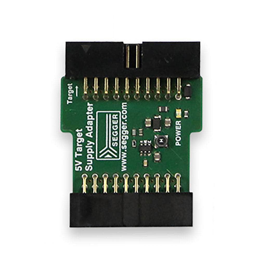
SEGGER 5V Target Supply Adapter
SEGGER 5V Target Supply Adapter
SKU: 8.06.29
Couldn't load pickup availability
Overview
Downloads
What it is
Compact inline adapter that injects a regulated 5 V supply into the standard 20‑pin ARM/JTAG ribbon, preserving a 1:1 pass‑through for all debug signals while powering the target from pin 19.
Where it fits
Plugs directly between any compatible SEGGER J‑Link or Flasher and the 20‑pin ribbon cable, adding a fixed 5 V target supply without extra wiring or bench supplies.
Key specifications
| Parameter | Value |
|---|---|
| Output voltage | 5 V ±5 % (fixed, delivered on pin 19) |
| Max output current | Up to 500 mA (limited by host); typical J‑Link yields ≈5 V/220 mA |
| Max capacitive load | 220 µF |
| Output ramp time | 2–6 ms |
| Connectors | 20‑pin 0.1″ socket (probe side) to 20‑pin 0.1″ header (target side) |
| Compatible hosts | J‑Link BASE/PLUS/ULTRA+/PRO/PRO PoE, WiFi, and Flashers |
Actual available current depends on the driving probe’s power capability; a typical J‑Link providing ~4.5 V/300 mA supports about 220 mA at 5 V.
Wiring quick‑start
- Power down the target and disconnect any existing target supply sources to avoid back‑feeding.
- Insert the adapter between the J‑Link/Flasher and the 20‑pin ribbon (socket to probe, header to cable).
- Connect the ribbon to the target’s 20‑pin ARM/JTAG header, ensuring pin‑1 orientation.
- Power the J‑Link/Flasher; the adapter will ramp 5 V to the target within 2–6 ms on pin 19.
- Verify target current draw stays within the host’s limit (typ. ~220 mA via standard J‑Link).
20‑pin ARM/JTAG pinout (adapter preserves 1:1 signals)
1: VTref 2: GND 3: nTRST 4: GND 5: TDI 6: GND 7: TMS/SWDIO 8: GND 9: TCK/SWCLK 10: GND 11: RTCK 12: GND 13: TDO/SWO 14: GND 15: nRESET 16: GND 17: DBGRQ 18: GND 19: +5V OUT 20: GND The adapter drives +5 V on pin 19; all other pins are pass‑through for standard JTAG/SWD signalling per ARM 20‑pin assignment.
Notes and cautions
- Do not parallel external supplies; power the target either from the adapter or an external regulator, not both.
- Large input capacitance above 220 µF may affect ramp behaviour or trip host limits.
- Output voltage can be altered by resistor changes at user risk; use SEGGER’s adjustable adapter (8.06.18) if routinely needing 0.8–3.6 V.
| General Information | |
|---|---|
Product Type |
Adapter
|
Part Number (SKU) |
8.06.29
|
Manufacturer |
|
| Physical and Mechanical | |
Weight |
0.02 kg
|
| Other | |
EAN |
5055383614271
|
Frequently Asked Questions
Have a Question?
Be the first to ask a question about this.