

Mikroelektronika d.o.o.
Scanner Click Board™
Scanner Click Board™
SKU: MIKROE-4108
Couldn't load pickup availability


Overview
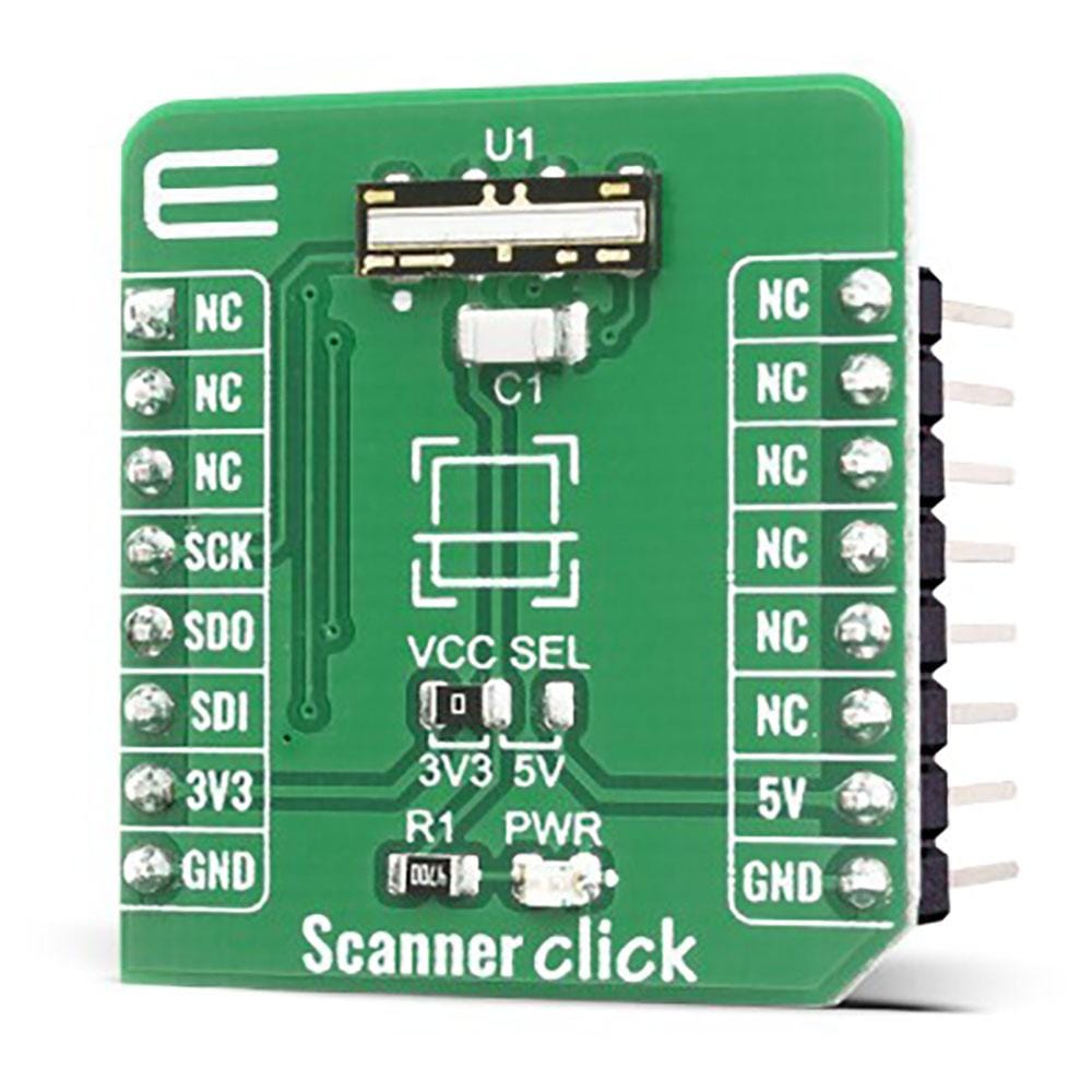
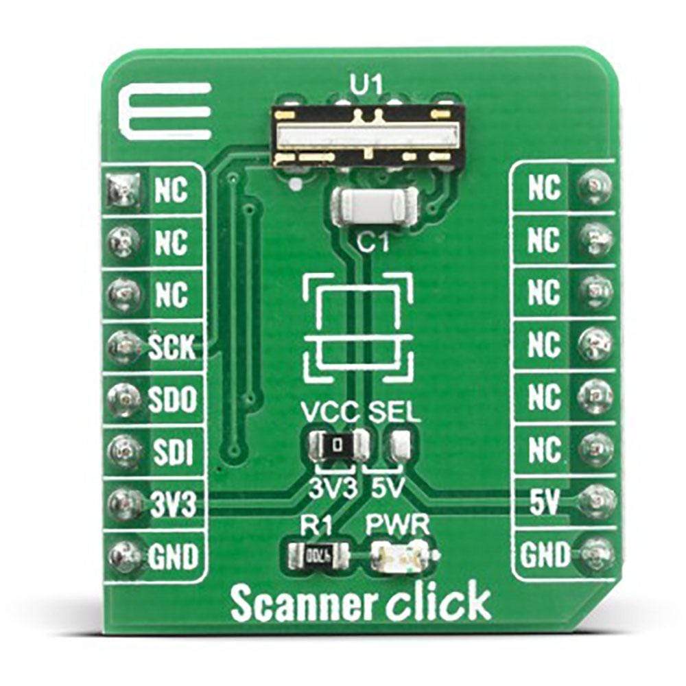
The Scanner Click Board™ is an optical scanner expansion board for building optical cost-sensitive scanners and printers. The main component of this board is a 102 pixels linear optical array sensor marked TSL3301CL from AMS. For accessing sensor registers from any host controller communication is accomplished through a three-wire SPI high-speed serial interface. This linear optical sensor provides high-density pixel count and integrated analogue-to-digital conversion to the Scanner Click Board™ and also enables high-resolution scanning and scalable operating range. This Click Board™ is most suitable for the applications like scanners, printer edge detects and optical character recognition.
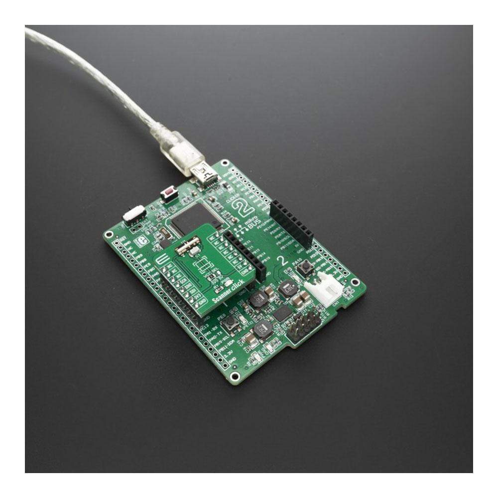
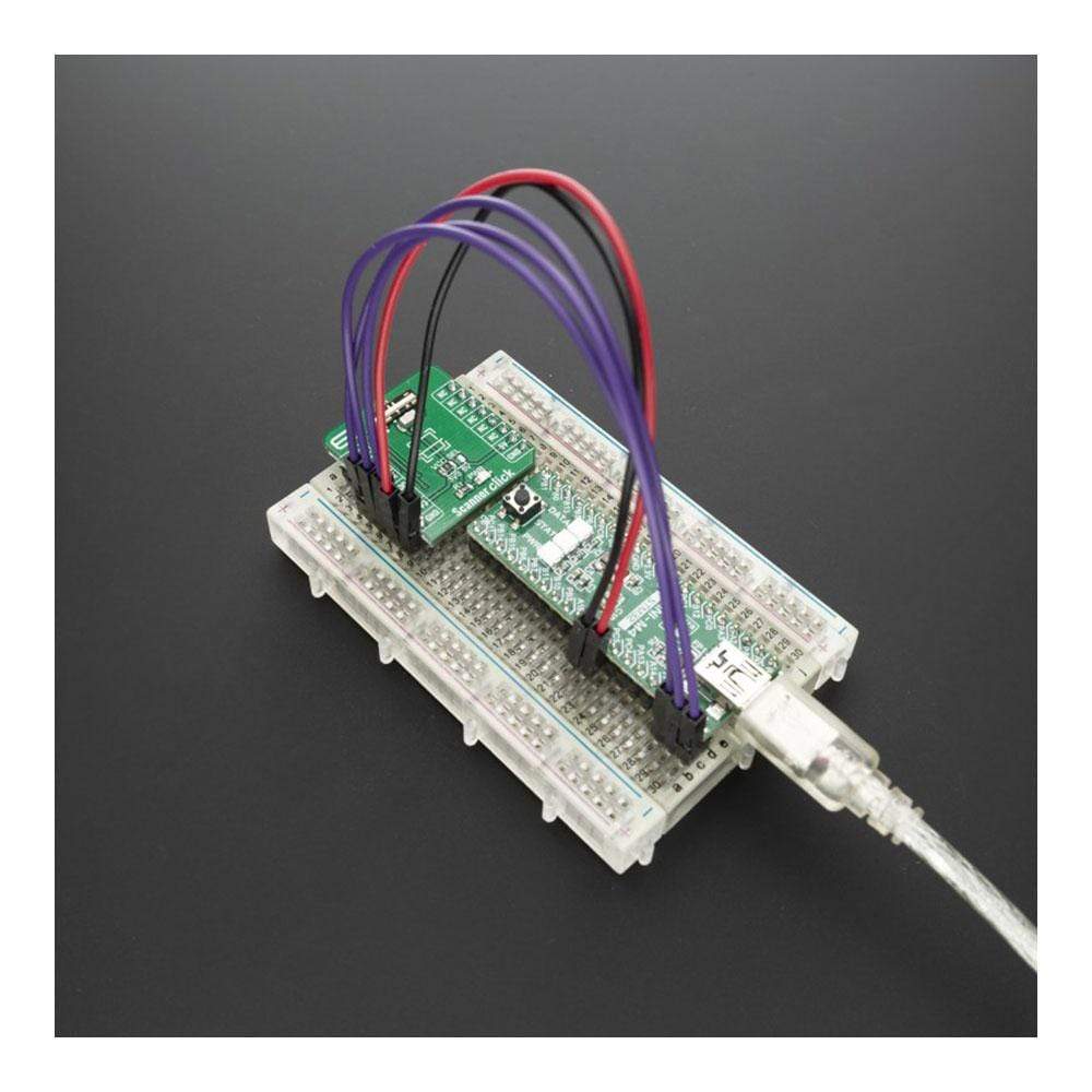
The Scanner Click Board™ is supported by a mikroSDK compliant library, which includes functions that simplify software development. This Click Board™ comes as a fully tested product, ready to be used on a system equipped with the mikroBUS™ socket.
Downloads
How Does The Scanner Click Board™ Work?
The Scanner Click Board™ uses the TSL3301CL IC, 102 × 1 linear optical sensor array with onboard A/D conversion from AMS-AG. The sensor consists of 102 photodiodes, also called pixels, arranged in a linear array. Light energy impinging on a pixel generates a photocurrent, which is then integrated by the active integration circuitry associated with that pixel. During the integration period, a sampling capacitor connects to the output of the integrator through an analog switch. The amount of charge accumulated at each pixel is directly proportional to the light intensity on that pixel and to the integration time. Integration, sampling, output, and reset of the integrators are performed by the control logic in response to commands input via the SDI serial data input pin on the mikroBUS™. Data is than read out on the SDO serial data output pin.

A normal sequence of operation consists of a pixel reset, start of integration, integration period, sampling of integrators, and pixel output. Reset sets all the integrators to zero. Start of integration releases the integrators from the reset state and defines the beginning of the integration period. Sampling the integrators ends the integration period and stores the charge accumulated in each pixel in a sample and hold circuit. Reading the pixels causes the sampled value of each pixel to be converted to 8-bit digital format and output on the SDO serial data output pin. All 102 pixels are output sequentially unless interrupted by an abort command or reset command.
Gain adjustment is controlled by three 5-bit DACs, one for each of the the three zones, while offset correction is controlled by three 8-bit sign-magnitude DACs and is performed in the analog domain prior to the digital conversion. There is a separate offset DAC for each of the three zones, where codes 0h - 7Fh correspond to positive offset values and codes 80h – FFh correspond to negative offset values. The programmed offset correction is applied to the sampled energy, and then the gain is applied (i.e. the gain will affect the offset correction).
The Scanner Click Board™ communicates over a serial digital interface (SPI serial interface) that follows a USART format, with start bit, 8 data bits, and one or more stop bits. Data is clocked in synchronously on the rising edge of system clock from SCK pin on the mikroBUS™ and clocked out on the falling edge of system clock. When clocking data out continuously (i.e. reading out pixels) there will be one stop bit between data words. The receive and transmit state machines are independent, which means commands can be issued while reading data. This feature allows starting new integration cycles while reading data.
It is designed to be operated with both 3.3V and 5V logic levels that can be selected via VCC SEL jumper. This allows for both 3.3V and 5V capable MCUs to use the SPI communication lines properly.
SPECIFICATIONS
| Type | Optical |
| Applications | Can be used for applications like scanners, printer edge detect and optical character recognition. |
| On-board modules | The Scanner Click Board™ uses the TSL3301CL IC, 102 × 1 linear optical sensor array with onboard A/D conversion from AMS-AG. |
| Key Features | High density 102 pixel count and integrated analog-to-digital conversion sensor, with high resolution scanning of 300dpi and scalable operating range |
| Interface | SPI |
| Compatibility | mikroBUS |
| Click board size | S (28.6 x 25.4 mm) |
| Input Voltage | 3.3V or 5V |
| Category | Click Boards |
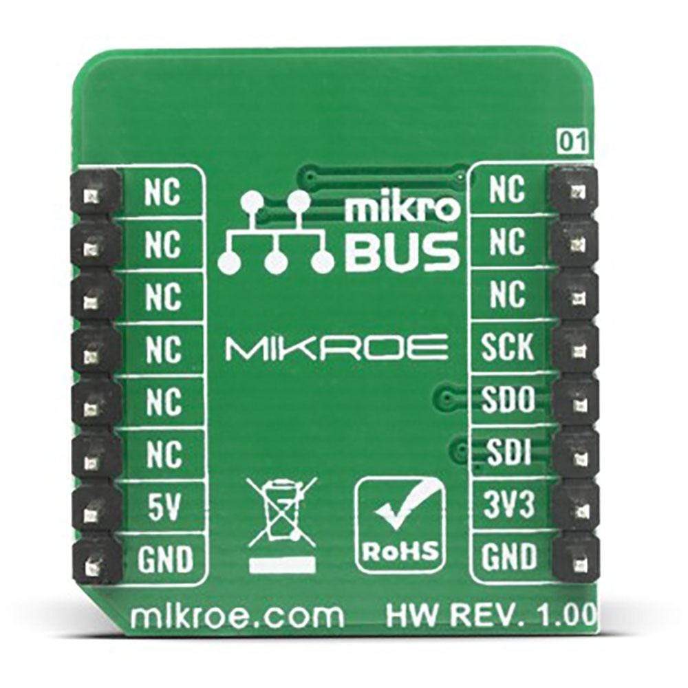
PINOUT DIAGRAM
This table shows how the pinout of the Scanner Click Board™ corresponds to the pinout on the mikroBUS™ socket (the latter shown in the two middle columns).
| Notes | Pin | Pin | Notes | ||||
|---|---|---|---|---|---|---|---|
| NC | 1 | AN | PWM | 16 | NC | ||
| NC | 2 | RST | INT | 15 | NC | ||
| NC | 3 | CS | RX | 14 | NC | ||
| SPI Clock | SCK | 4 | SCK | TX | 13 | NC | |
| SPI Data OUT | SDO | 5 | MISO | SCL | 12 | NC | |
| SPI Data IN | SDI | 6 | MOSI | SDA | 11 | NC | |
| Power Supply | 3.3V | 7 | 3.3V | 5V | 10 | 5V | Power Supply |
| Ground | GND | 8 | GND | GND | 9 | GND | Ground |
ONBOARD SETTINGS AND INDICATORS
| Label | Name | Default | Description |
|---|---|---|---|
| LD1 | PWR | - | Power LED Indicator |
| JP1 | VCC SEL | Left | Power Supply Voltage Selection 3V3/5V, left position 3V3, right position 5V |
SCANNER CLICK ELECTRICAL SPECIFICATIONS
| Description | Min | Typ | Max | Unit |
|---|---|---|---|---|
| Supply Voltage | +6 | V | ||
| Maximum Output Current | -10 | +10 | mA | |
| Operating Temperature Range | -25 | +85 | °C | |
| Maximum Clock Frequency | 10 | MHz |
| General Information | |
|---|---|
Part Number (SKU) |
MIKROE-4108
|
Manufacturer |
|
| Physical and Mechanical | |
Weight |
0.02 kg
|
| Other | |
EAN |
8606018717552
|
Frequently Asked Questions
Have a Question?
Be the first to ask a question about this.