


Mikroelektronika d.o.o.
Boost Click Board™
Boost Click Board™
SKU: MIKROE-2780
Couldn't load pickup availability

Overview
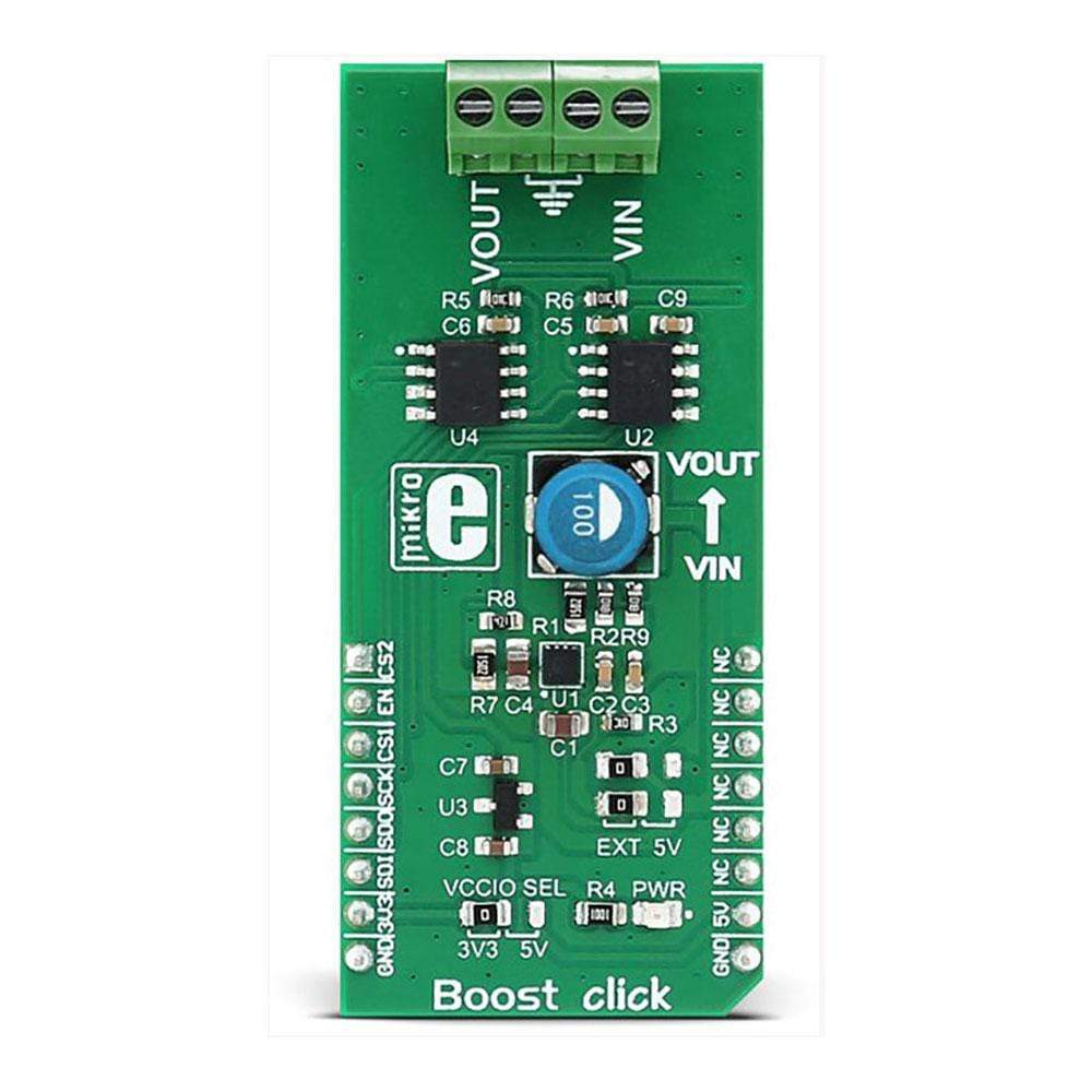
The Boost Click Board™ is based on Microchip's MIC2606, a 2MHz, PWM DC/DC boost switching regulator available in a 2mm x 2mm MLF package.
The Boost Click Board™ provides an adjustable output voltage through the onboard DAC that drives the FB pin of the MIC2606 to set the desired output voltage. The Click Board™ also has an onboard ADC that converts output voltage and sends its digital value through SPI pins of mikroBUS to the microcontroller.
Downloads
Boost Click Board™
The Boost Click Board™ carries Microchip's MIC2606, a 2MHz, PWM DC/DC boost switching regulator available in a 2mm x 2mm MLF® package.
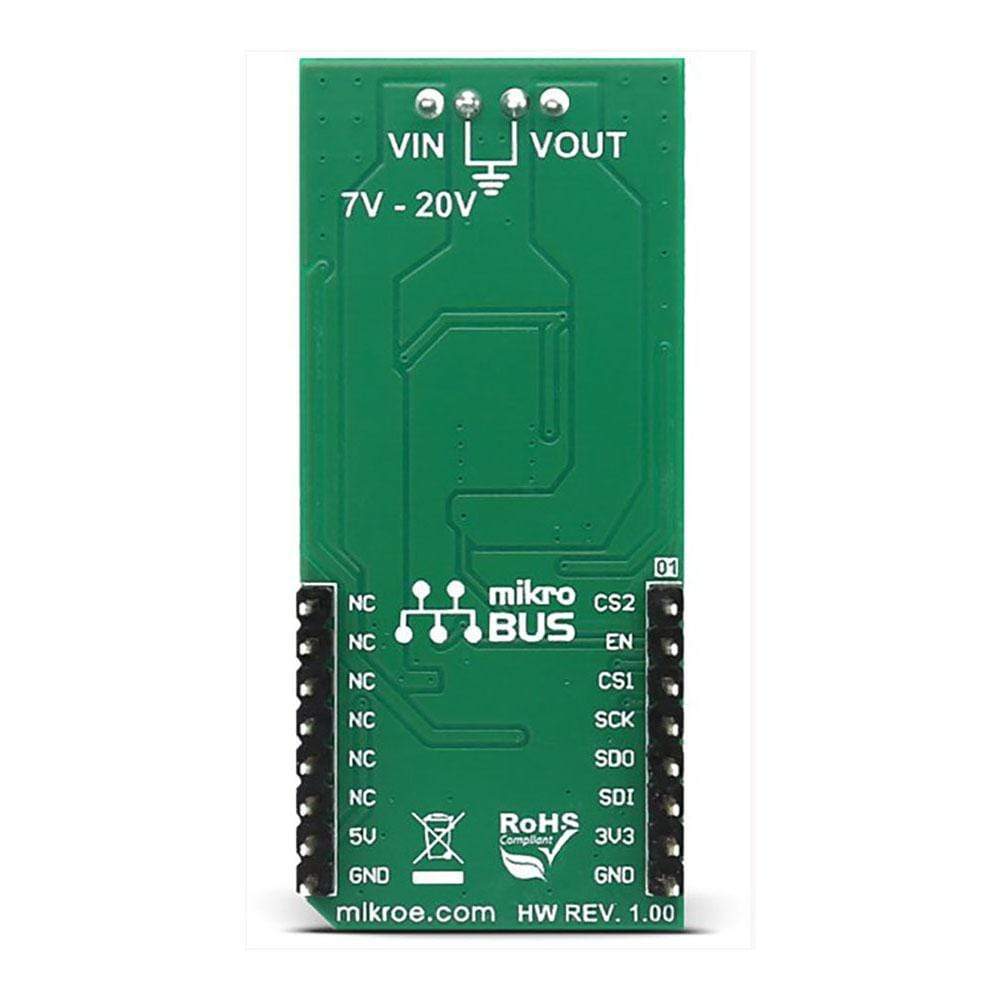
The Boost Click Board™ provides an adjustable output voltage through the onboard DAC that drives the FB pin of the MIC2606 to set desired output voltage. The click also has an onboard ADC that converts output voltage and sends its digital value through SPI pins of mikroBUS™ to the microcontroller. The input voltage can be set to 5V from mikroBUS™ or in range 7-20V from an external DC source connected to VIN screw terminal. The output voltage can be set up to 38V.
Note : If the user wants to connect external voltage to VIN, then the click needs the power supply unit connected to the VIN screw terminal.
How Does The Boost Click Board™ Work?
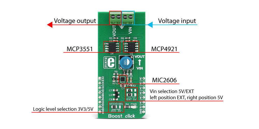
As you can see from the image there are two onboard screw terminals . One is for connecting the external VIN and the other is for connecting the load. The microcontroller reads the output voltage through the SPI from the onboard ADC and according to the desired output voltage, sends calculated data through SPI to an onboard DAC.
The DAC drives the FB pin of the MIC2606 to set desired output voltage. The output voltage must always be set greater than the input voltage, otherwise, performance is not guaranteed. Instead of connecting external VIN it is possible to use 5V from mikroBUS. This is done by changing the positions of two onboard jumpers from position EXT to position 5V.
Note: Both of them must be in position 5V, otherwise performance is not guaranteed.
Features
The MIC2606 is a 0.5A, 2MHz Wide Input Range Boost Regulator with Integrated Switch and Schottky Diode. It's FB (feedback) pin provides the control path to control the output. This FB pin is driven by an onboard DAC – MCP4921. This is a 2.7 – 5.5V, low-power, low DNL, 12-Bit Digital-to-Analog Converter (DAC) with SPI interface. It provides high accuracy and low noise performance for industrial applications. The output voltage is connected to an onboard ADC - MCP3551 - through a voltage divider. MCP3551 is a 2.7V to 5.5V low-power, 22-bit Delta-Sigma Analog-to-Digital Converter.
The reference voltage for both the ADC and DAC is provided by MAX6106 – onboard voltage reference.
Specifications
| Type | Boost |
| Applications | Any applications where it is necessary to step up the voltage |
| On-board modules | MIC2606, MCP3551, MCP4921 |
| Key Features | the 0.5A, 2MHz Wide Input Range Boost Regulator with Integrated Switch and Schottky Diode, high accuracy and low noise performance |
| Interface | SPI |
| Compatibility | mikroBUS |
| Click board size | L (57.15 x 25.4 mm) |
| Input Voltage | 3.3V or 5V |
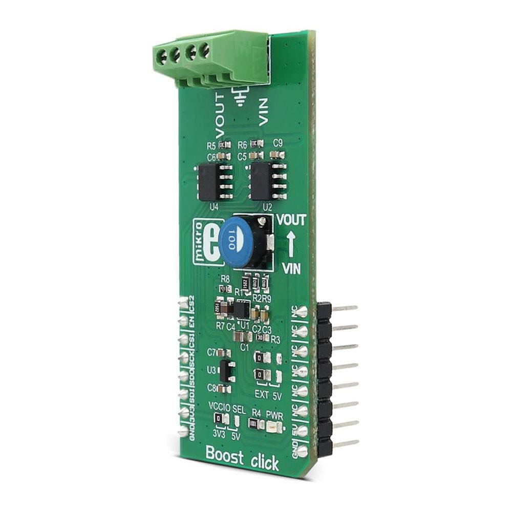
Pinout Diagram
This table shows how the pinout on the Boost Click Board™ corresponds to the pinout on the mikroBUS™ socket (the latter shown in the two middle columns).
| Notes | Pin | Pin | Notes | ||||
|---|---|---|---|---|---|---|---|
| DAC chip select | CS2 | 1 | AN | PWM | 16 | NC | |
| MIC2606 enable | EN | 2 | RST | INT | 15 | NC | |
| ADC chip select | CS1 | 3 | CS | TX | 14 | NC | |
| SPI clock pin | SCK | 4 | SCK | RX | 13 | NC | |
| SPI slave data out pin | SDO | 5 | MISO | SCL | 12 | NC | |
| SPI slave data in pin | SDI | 6 | MOSI | SDA | 11 | NC | |
| Power supply | +3.3V | 7 | 3.3V | 5V | 10 | +5V | Power supply |
| Ground | GND | 8 | GND | GND | 9 | GND | Ground |
Jumpers and settings
| Designator | Name | Default Position | Default Option | Description |
|---|---|---|---|---|
| JP1 | VCCIO SEL | Left | 3V3 | Logic level selection 3V3/5V, left position 3V3, right position 5V |
| JP2 | VIN SEL | Left | EXT | Vin selection 5V/EXT, left position EXT, right position 5V |
| JP3 | VIN SEL | Left | EXT | Vin selection 5V/EXT, left position EXT, right position 5V |
JP1 - this jumper allows you to select the logic level voltage for the communication lines. It can be 3.3V or 5V and must be paired with the supply voltage of the host microcontroller.
JP2 and JP3 - these jumpers serve to select the input voltage of the MIC2606. Both jumpers must always be in the same position and move simultaneously. If they are in the left position, (EXT) then the input voltage is taken from the connector VIN, if they are in the right position, (5V) then the input voltage is taken from the mikroBUS™ and it is 5V.
Maximum ratings
| Description | Min | Typ | Max | Unit |
|---|---|---|---|---|
| VIN | 7 (1) | ... | 20 (1) | V |
| 5 (2) | ||||
| VOUT | 15 (1) | ... | 38 | V |
| 12 (2) | ... | 38 |
(1) If external supply is connected
(2) If V IN is 5V from mikroBUS
| General Information | |
|---|---|
Part Number (SKU) |
MIKROE-2780
|
Manufacturer |
|
| Physical and Mechanical | |
Weight |
0.025 kg
|
| Other | |
EAN |
8606018711611
|
Frequently Asked Questions
Have a Question?
Be the first to ask a question about this.