2x2 Key Click Board
2x2 Key Click Board
Overview
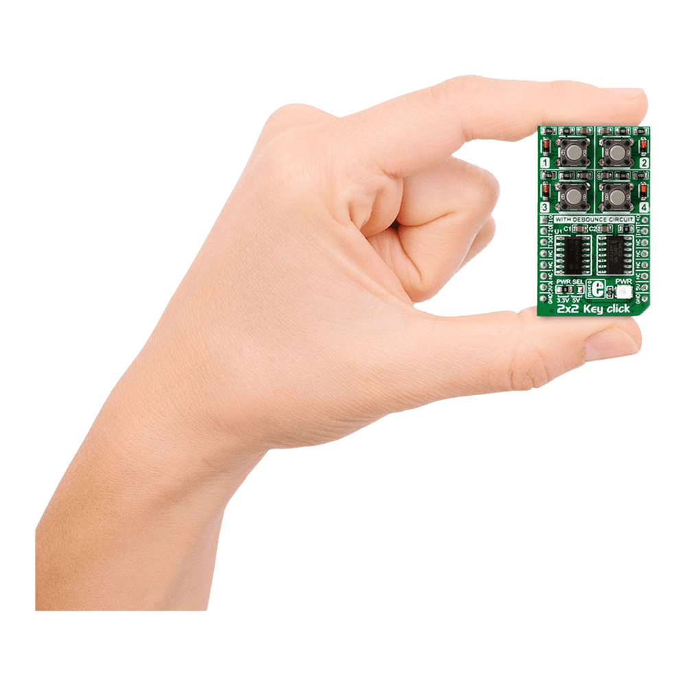
Discover the versatility and functionality of the 2x2 Key Click Board™, a cutting-edge solution for your keypad needs. Designed to offer seamless integration and reliable performance, this innovative board caters to a wide range of applications with its advanced features and intuitive design.
When you choose the 2x2 Key Click Board™, you unlock a world of possibilities. Whether you are a hobbyist or a professional, this versatile keypad solution is tailored to meet your specific requirements with precision and efficiency.
- Experience seamless multi-key functionality with the 2x2 Key Click Board™, designed to support multiple key presses effortlessly.
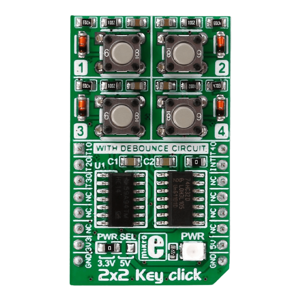
- Benefit from enhanced durability and responsiveness thanks to the debounce circuit featuring top-quality components from leading manufacturers like NXP and Texas Instruments.
Engineered to adapt to various power supply configurations, the 2x2 Key Click Board™ is compatible with both 3.3V and 5V power sources, ensuring flexibility and convenience in your projects.
With independent button reading capability, this Click Board™ offers enhanced control and precision, allowing you to customise your key inputs according to your specific requirements.
Explore the seamless integration and unparalleled performance of the 2x2 Key Click Board™, a reliable and versatile solution for all your keypad needs. Elevate your projects to new heights with this cutting-edge keypad solution that combines innovation with reliability and efficiency.
Embrace the future of keypad technology with the 2x2 Key Click Board™ - your gateway to seamless key input solutions for a wide range of applications. Unlock the potential of your projects with this advanced Click Board™ that promises precision, reliability, and flexibility in every keystroke.
DEBOUNCE CIRCUIT
In electronics, two metal components tend to bounce or create multiple signals when they are in contact with each other — like when you push a button — before they get to a stable state. You want a single contact to be recorded, but the microcontroller records this as if you pressed the button many times.
So debouncing is, as the name states, the removal of bounces or spikes of low and high voltages. Graphically speaking, you want a clean line, not spikes. A debounce circuit makes sure that there are no voltage changes on the output. Thanks to it, one button press is recorded as such.
INTERRUPT SERVICE ROUTINE
All four Schmitt-trigger outputs are connected to input pins of the logic OR gate 74HC32, whose output is directly connected to the INT pin on mikroBUS. This pin is used to signalize an interrupt to the MCU any time a button is pressed.
In this way, the MCU software can be implemented as a simple polling routine, without any delays programmed in the code (like it would be necessary if there wasn't a hardware debouncing circuit present).
Thanks to the INT pin you can easily program a common interrupt service routine, in order to detect when a button is pressed (the state of the button changes from low to high logic level).
SPECIFICATIONS
Type | Pushbutton/Switches |
Applications | Human machine interface applications |
On-board modules | 74HC32 quad 2-input OR gate from NXP and the SN74HC14 Hex Schmitt-Trigger Inverter from Texas Instruments |
Key Features | 74HC32 quad 2-input OR gate, SN74HC14 Hex Schmitt-Trigger Inverte |
Interface | GPIO |
Compatibility | mikroBUS |
Click board size | M (42.9 x 25.4 mm) |
Input Voltage | 3.3V or 5V |
ADDITIONAL INFORMATION
- J2 is the interrupt enable pin (by default it is in the enable status).
- J1 is the power selection pin.
PINOUT DIAGRAM
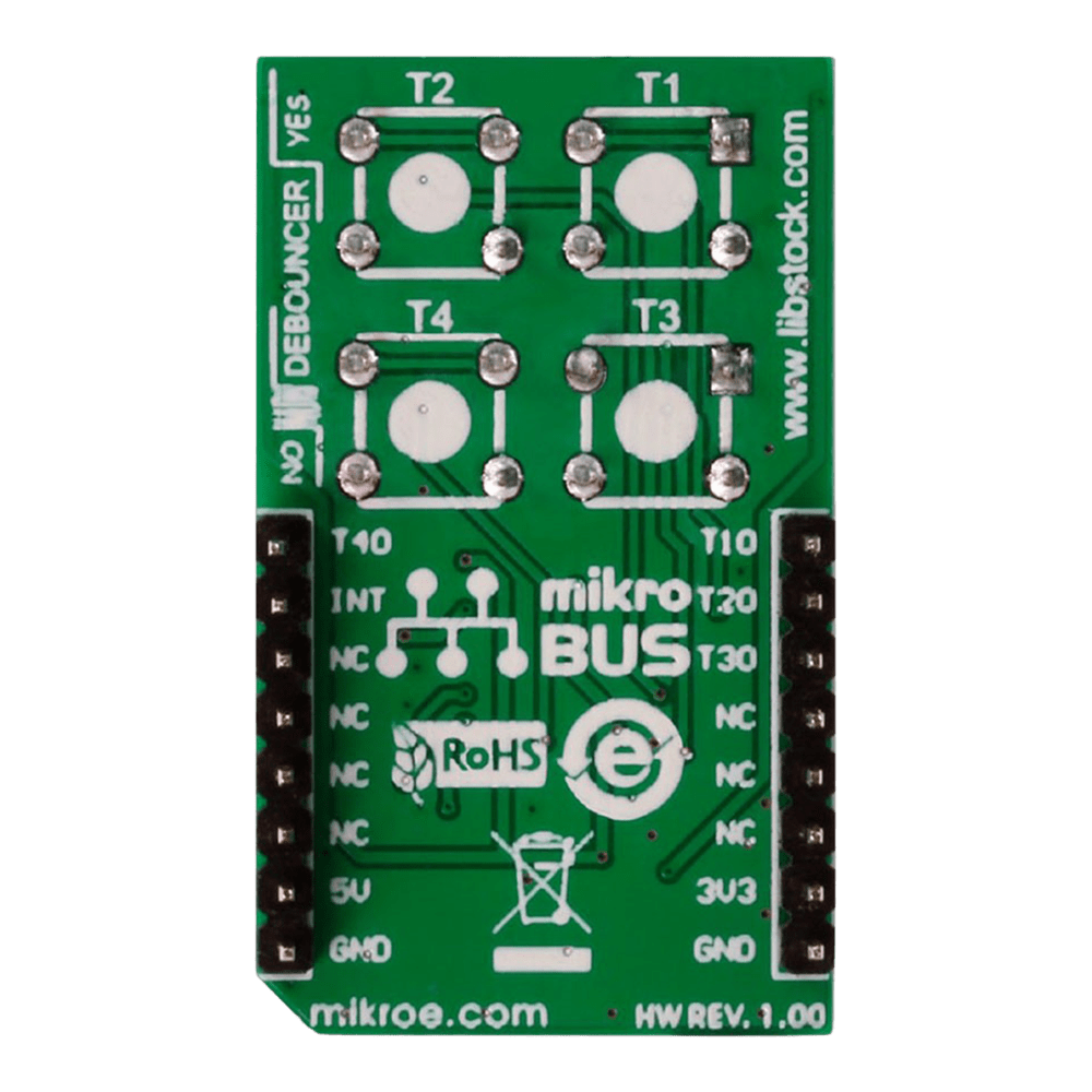
This table shows how the pinout on 2x2 Key click corresponds to the pinout on the mikroBUS™ socket (the latter shown in the two middle columns).
Notes | Pin | Pin | Notes | ||||
---|---|---|---|---|---|---|---|
When button T1 is pressed the pin is active | T1-OUT | 1 | AN | PWM | 16 | T4-OUT | When button T4 is pressed the pin is active |
When button T2 is pressed the pin is active | T2-OUT | 2 | RST | INT | 15 | TINT | Interrupt pin that notifies the MCU that a button is pressed |
When button T3 is pressed the pin is active | T3-OUT | 3 | CS | TX | 14 | NC | |
NC | 4 | SCK | RX | 13 | NC | ||
NC | 5 | MISO | SCL | 12 | NC | ||
NC | 6 | MOSI | SDA | 11 | NC | ||
Power supply | +3.3V | 7 | 3.3V | 5V | 10 | +5V | Power supply |
Ground | GND | 8 | GND | GND | 9 | GND | Ground |
Software Support
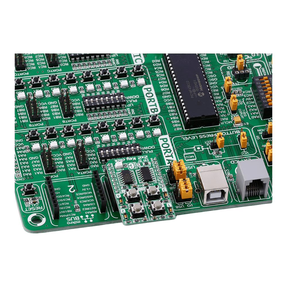
The demo initialises the TFT display and sets pins to operate in input direction. The main function of the demo uses the polling method to check if inputs are on an active level. The TFT display shows the button state according to detect level.
1 void main() 2 { 3 system_init(); 4 5 Draw_Taster(X1, Y1, RELEASED, "T1"); 6 Draw_Taster(X2, Y1, RELEASED, "T2"); 7 Draw_Taster(X1, Y2, RELEASED, "T3"); 8 Draw_Taster(X2, Y2, RELEASED, "T4"); 9 10 while(1) 11 { 12 if(Taster_Pressed(TAST1, &t1_state)) 13 Draw_Taster(X1, Y1, PRESSED, "T1"); 14 15 if(Taster_Released(TAST1, &t1_state)) 16 Draw_Taster(X1, Y1, RELEASED, "T1"); 17 18 if(Taster_Pressed(TAST2, &t2_state)) 19 Draw_Taster(X2, Y1, PRESSED, "T2"); 20 21 if(Taster_Released(TAST2, &t2_state)) 22 Draw_Taster(X2, Y1, RELEASED, "T2"); 23 24 if(Taster_Pressed(TAST3, &t3_state)) 25 Draw_Taster(X1, Y2, PRESSED, "T3"); 26 27 if(Taster_Released(TAST3, &t3_state)) 28 Draw_Taster(X1, Y2, RELEASED, "T3"); 29 30 if(Taster_Pressed(TAST4, &t4_state)) 31 Draw_Taster(X2, Y2, PRESSED, "T4"); 32 33 if(Taster_Released(TAST4, &t4_state)) 34 Draw_Taster(X2, Y2, RELEASED, "T4"); 35 36 t1_state = TAST1; 37 t2_state = TAST2; 38 t3_state = TAST3; 39 t4_state = TAST4; 40 41 Delay_ms(POLLING_PERIOD); 42 } 43 }
Frequently Asked Questions
Have a Question?
Be the first to ask a question about this.
Details
DEBOUNCE CIRCUIT
In electronics, two metal components tend to bounce or create multiple signals when they are in contact with each other — like when you push a button — before they get to a stable state. You want a single contact to be recorded, but the microcontroller records this as if you pressed the button many times.
So debouncing is, as the name states, the removal of bounces or spikes of low and high voltages. Graphically speaking, you want a clean line, not spikes. A debounce circuit makes sure that there are no voltage changes on the output. Thanks to it, one button press is recorded as such.
INTERRUPT SERVICE ROUTINE
All four Schmitt-trigger outputs are connected to input pins of the logic OR gate 74HC32, whose output is directly connected to the INT pin on mikroBUS. This pin is used to signalize an interrupt to the MCU any time a button is pressed.
In this way, the MCU software can be implemented as a simple polling routine, without any delays programmed in the code (like it would be necessary if there wasn't a hardware debouncing circuit present).
Thanks to the INT pin you can easily program a common interrupt service routine, in order to detect when a button is pressed (the state of the button changes from low to high logic level).
SPECIFICATIONS
Type | Pushbutton/Switches |
Applications | Human machine interface applications |
On-board modules | 74HC32 quad 2-input OR gate from NXP and the SN74HC14 Hex Schmitt-Trigger Inverter from Texas Instruments |
Key Features | 74HC32 quad 2-input OR gate, SN74HC14 Hex Schmitt-Trigger Inverte |
Interface | GPIO |
Compatibility | mikroBUS |
Click board size | M (42.9 x 25.4 mm) |
Input Voltage | 3.3V or 5V |
ADDITIONAL INFORMATION
- J2 is the interrupt enable pin (by default it is in the enable status).
- J1 is the power selection pin.
PINOUT DIAGRAM
This table shows how the pinout on 2x2 Key click corresponds to the pinout on the mikroBUS™ socket (the latter shown in the two middle columns).
Notes | Pin | Pin | Notes | ||||
---|---|---|---|---|---|---|---|
When button T1 is pressed the pin is active | T1-OUT | 1 | AN | PWM | 16 | T4-OUT | When button T4 is pressed the pin is active |
When button T2 is pressed the pin is active | T2-OUT | 2 | RST | INT | 15 | TINT | Interrupt pin that notifies the MCU that a button is pressed |
When button T3 is pressed the pin is active | T3-OUT | 3 | CS | TX | 14 | NC | |
NC | 4 | SCK | RX | 13 | NC | ||
NC | 5 | MISO | SCL | 12 | NC | ||
NC | 6 | MOSI | SDA | 11 | NC | ||
Power supply | +3.3V | 7 | 3.3V | 5V | 10 | +5V | Power supply |
Ground | GND | 8 | GND | GND | 9 | GND | Ground |