


Mikroelektronika d.o.o.
Multi Stepper TB67S209 Click Board™
Multi Stepper TB67S209 Click Board™
SKU: MIKROE-5042
Couldn't load pickup availability

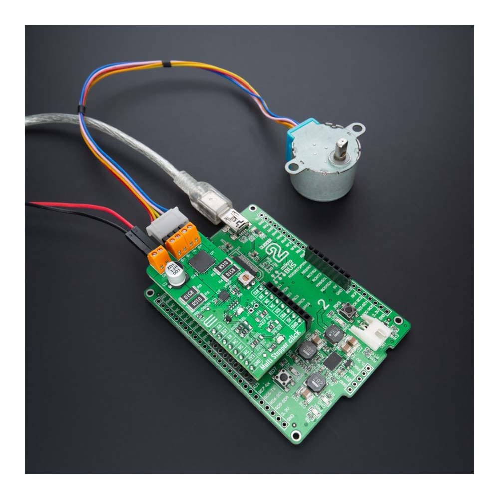
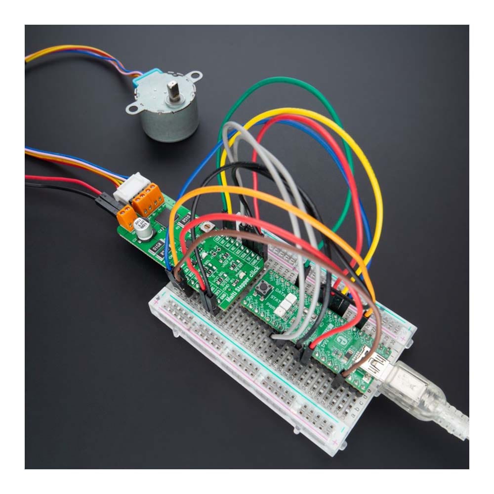
Overview
The Multi Stepper TB67S209 Click Board™ is a compact add-on board that contains a bipolar stepper motor driver. This board features the TB67S209FTG, CLOCK-in controlled bipolar stepping motor driver from Toshiba Semiconductor. It supports a PWM constant-current control drive, selectable mixed decay mode, and allows from full-step up to 1/32 steps resolution for less motor noise and smoother control. It has a wide operating voltage range of 10V to 47V with an output current capacity of 2.8A in addition to several built-in error detection circuits. This Click board™ makes the perfect solution for stepping motors in various applications such as office automation, commercial, and industrial equipment.
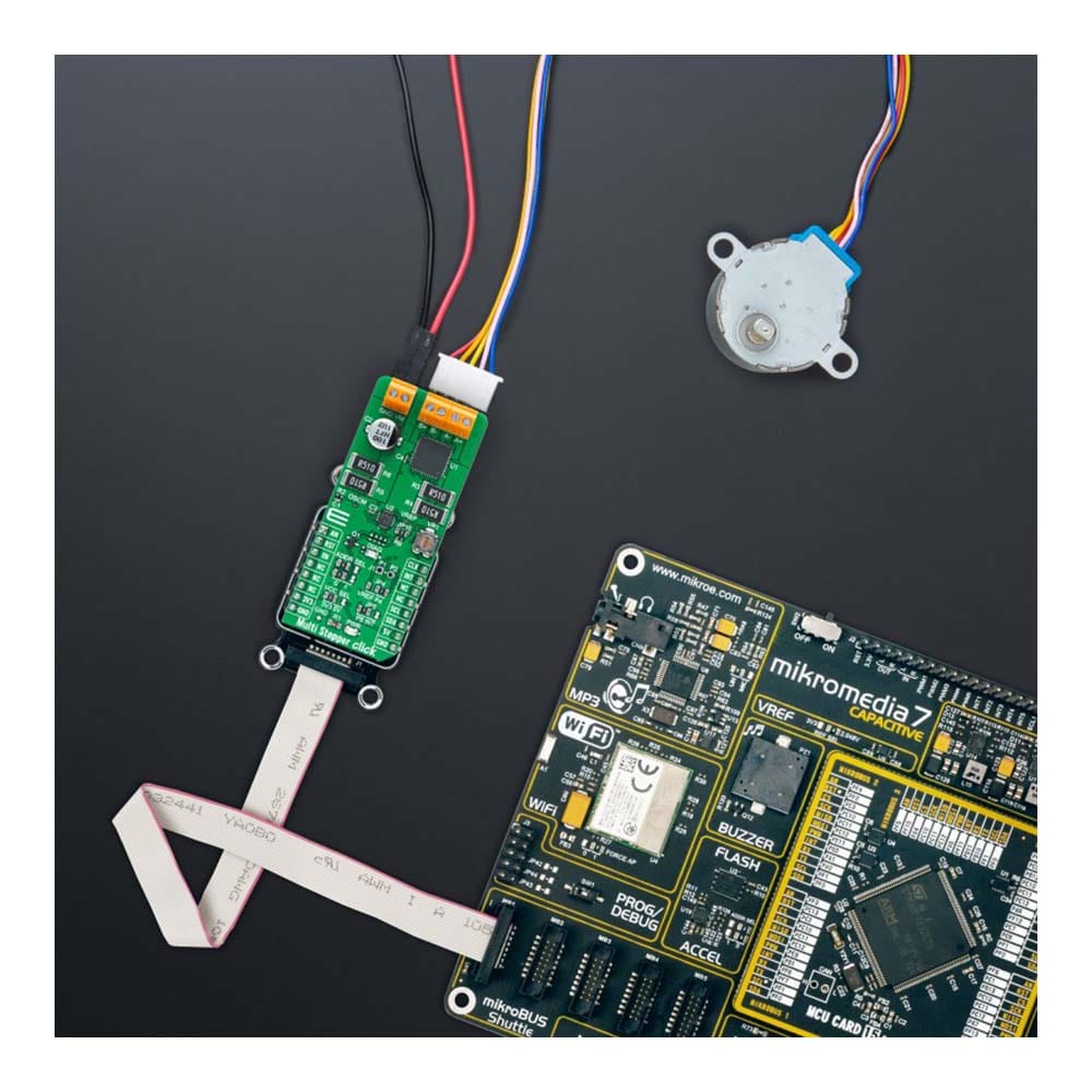
The Multi Stepper TB67S209 Click Board™ is supported by a mikroSDK compliant library, which includes functions that simplify software development. This Click board™ comes as a fully tested product, ready to be used on a system equipped with the mikroBUS™ socket.
Downloads
How Does The Multi Stepper TC67S209 Click Board™ Work?
The Multi Stepper TC67S209 Click Board™ is based on the TB67S209FTG, a two-phase bipolar stepping motor driver using a PWM chopper from Toshiba Semiconductor. The TB67S209FTG comes with a built-in clock-in decoder (CLOCK-in controlled), which means that each up-edge of the CLK signal, routed to the PWM pin of the mikroBUS™ socket, will shift the motor's electrical angle per step. It also incorporates a low on-resistance MOSFET output stage, which can deliver a 2.8A current with a motor output voltage rating of 47V, in addition to integrated protection mechanisms such as over-current, over-temperature, and under-voltage detection. In addition, it allows from full-step up to 1/32 steps resolution, with the help of which motor noise can be significantly reduced with smoother operation and more precise control.
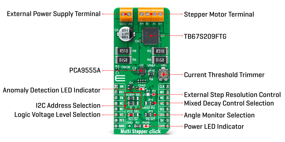
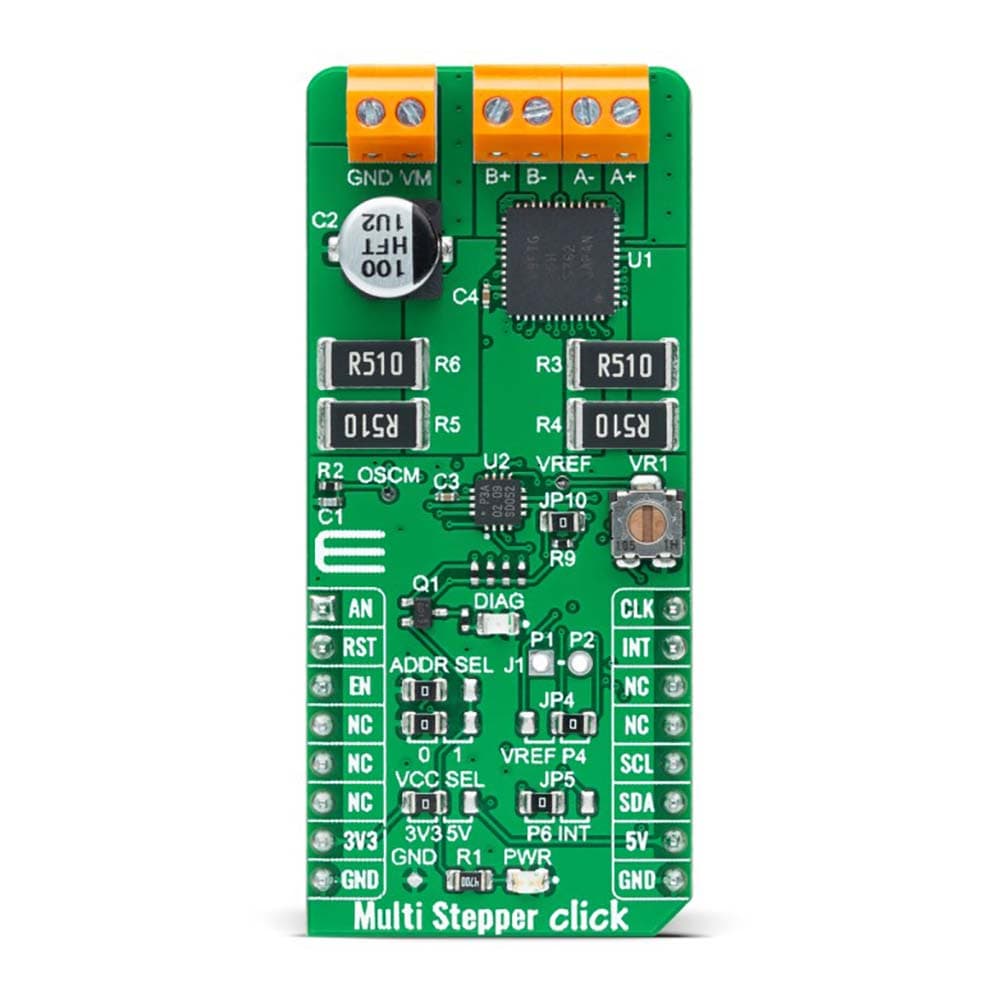
The TB67S209FTG supports selectable Mixed Decay mode. Though the Mixed Decay is determined by controlling two different types of decay (Fast Decay and Slow Decay), this function enables the user to select the ration of the Mixed Decay through the PCA9555A pins P4/P5. To allow both pins to be configurated by the expander, the SMD jumper labelled as JP4 must be positioned to an appropriate position marked as P4. Also, the motor current output value can be set manually using an onboard trimmer labelled as VR1, which sets the reference voltage in the range from 0V to 3.3V.
As mentioned before, the TB67S209FTG supports various step resolution configurations through its control signals. These control signals are provided through the PCA9555A port expander, which establishes communication with the MCU via the I2C serial interface. This Click board™ also allows a connection of external step-resolution control signals on the onboard header J1 on pins labelled as P1 and P2 for the device's DMODE1 and DMODE2 control. The PCA9555A also allows choosing the least significant bit (LSB) of its I2C slave address by positioning SMD jumpers labelled as ADDR SEL to an appropriate position marked as 0 and 1.
Also, the Multi Stepper TC67S209 Click Board™ has a Standby function, activated when all three step-resolution control signals are on its low logic state, used to switch to Standby mode by setting all motor control pins to a low logic state. When the Standby mode is active, the TB67S209FTG stops supplying the power to the internal oscillating circuit and motor output part (the motor drive cannot be performed).
In addition to the I2C communication, several GPIO pins connected to the mikroBUS™ socket are also used. The Enable pin, labelled as EN and routed to the CS pin of the mikroBUS™ socket, optimizes power consumption used for power ON/OFF purposes. Also, a simple rotation direction function routed to the AN pin on the mikroBUS™ socket allows MCU to manage the direction of the stepper motor (clockwise or counterclockwise), while the RST pin of the mikroBUS™ socket initializes an electrical angle in the internal counter to set an initial position.
When it comes to angle monitoring, this Click board™ has a dual way of monitoring selected by positioning SMD jumper labelled as JP5 to an appropriate position marked as P6 or INT, which choose to monitor via expander or INT pin of the mikroBUS™ socket. In that case, such anomaly is indicated by a red LED marked as DIAG and via P7 pin over the I2C INT to the mikroBUS™ INT pin proceeding JP5 is set to P6.
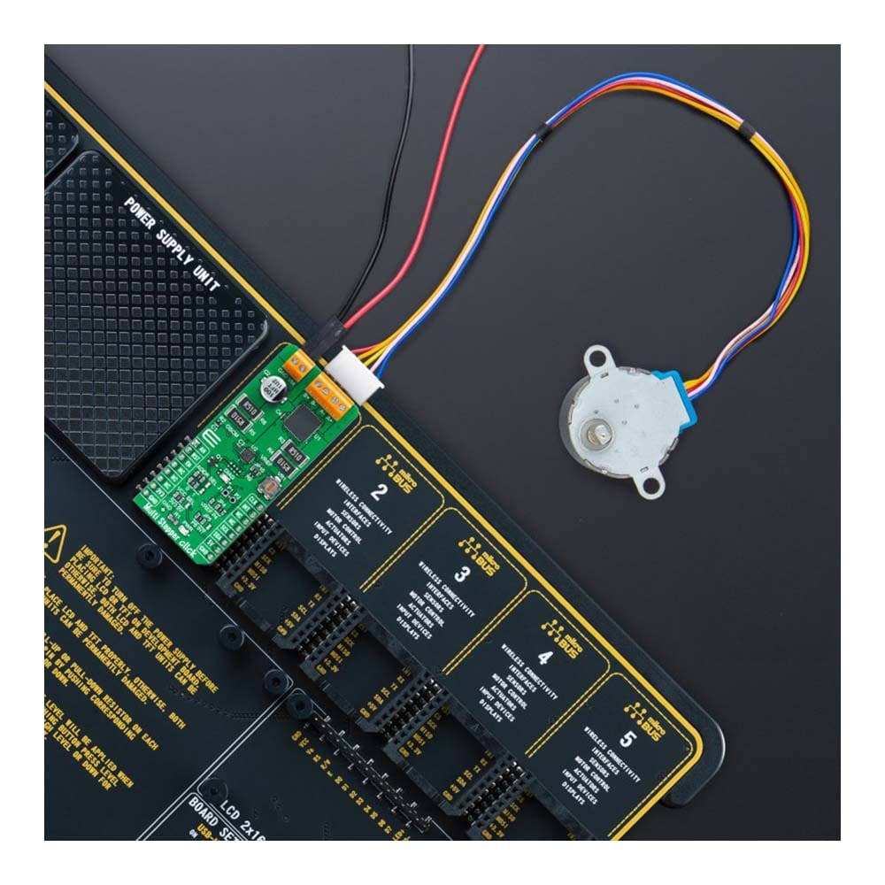
The Multi Stepper TC67S209 Click Board™ supports an external power supply for the TB67S209FTG, which can be connected to the input terminal labelled as VM and should be within the range of 10V to 47V, while the stepper motor coils can be connected to the terminals labelled as B+, B-, A-, and A+.
The Multi Stepper TC67S209 Click Board™ can operate with both 3.3V and 5V logic voltage levels selected via the VCC SEL jumper. This way, it is allowed for both 3.3V and 5V capable MCUs to use communication lines properly. However, the Click board™ comes equipped with a library containing easy-to-use functions and an example code that can be used, as a reference, for further development.
SPECIFICATIONS
| Type | Stepper |
| Applications | The Multi Stepper TC67S209 Click Board™ can be used for stepping motors in various applications such as office automation, commercial, and industrial equipment |
| On-board modules | TB67S209FTG - CLOCK-in controlled bipolar stepping motor driver from Toshiba Semiconductor |
| Key Features | Low power consumption, capable of controlling 1 bipolar stepping motor, from full-step up to 1/32 steps resolution, built-in clock decoder, selectable mixed decay mode, integrated error detection circuits, and more |
| Interface | GPIO,I2C |
| Compatibility | mikroBUS |
| Click board size | L (57.15 x 25.4 mm) |
| Input Voltage | External,3.3V or 5V |
PINOUT DIAGRAM
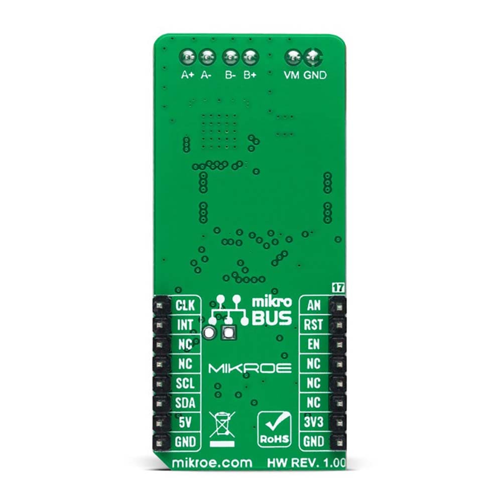
This table shows how the pinout of the Multi Stepper TC67S209 Click Board™ corresponds to the pinout on the mikroBUS™ socket (the latter shown in the two middle columns).
| Notes | Pin |  |
Pin | Notes | |||
|---|---|---|---|---|---|---|---|
| Rotation Direction | AN | 1 | AN | PWM | 16 | CLK | Clock Signal |
| Reset | RST | 2 | RST | INT | 15 | INT | Interrupt |
| Enable | EN | 3 | CS | RX | 14 | NC | |
| NC | 4 | SCK | TX | 13 | NC | ||
| NC | 5 | MISO | SCL | 12 | SCL | I2C Clock | |
| NC | 6 | MOSI | SDA | 11 | SDA | I2C Data | |
| Power Supply | 3.3V | 7 | 3.3V | 5V | 10 | 5V | Power Supply |
| Ground | GND | 8 | GND | GND | 9 | GND | Ground |
ONBOARD SETTINGS AND INDICATORS
| Label | Name | Default | Description |
|---|---|---|---|
| LD1 | PWR | - | Power LED Indicator |
| LD2 | DIAG | - | Anomaly Detection LED Indicator |
| JP1-JP2 | ADDR SEL | Left | I2C Address Selection 0/1: Left position 0, Right position 1 |
| JP3 | VCC SEL | Left | Logic Level Voltage Selection 3V3/5V: Left position 3V3, Right position 5V |
| JP4 | JP4 | Right | Mixed Decay Mode Control Selection VREF/P4: Left position VREF, Right position P4 |
| JP5 | JP5 | Left | Angle Monitoring Selection P6/INT: Left position P6, Right position INT |
| JP10 | JP10 | Populated | Angle Monitoring via Expander |
| J1 | J1 | Unpopulated | External Step Resolution Signals Connection Header |
| VR1 | VR1 | - | Current Threshold Trimmer |
| TP1 | VREF | - | Voltage Reference Testpoint |
| TP2 | OSCM | - | Oscillating Circuit Crequency Testpoint |
| TP3 | GND | - | Ground Testpoint |
MULTI STEPPER CLICK - TB67S209 ELECTRICAL SPECIFICATIONS
| Description | Min | Typ | Max | Unit |
|---|---|---|---|---|
| Supply Voltage VCC | 3.3 | - | 5 | V |
| External Supply Voltage VM | 10 | 24 | 47 | V |
| Motor Output Current | - | 2.8 | - | A |
| Motor Output Voltage | 10 | - | 47 | V |
| Operating Temperature Range | -20 | +25 | +85 | °C |
| General Information | |
|---|---|
Part Number (SKU) |
MIKROE-5042
|
Manufacturer |
|
| Physical and Mechanical | |
Weight |
0.02 kg
|
| Other | |
EAN |
8606027389184
|