


Mikroelektronika d.o.o.
Flash 10 Click-Platine
Flash 10 Click-Platine
SKU: MIKROE-5289
Verfügbarkeit für Abholungen konnte nicht geladen werden
Key Features
Overview
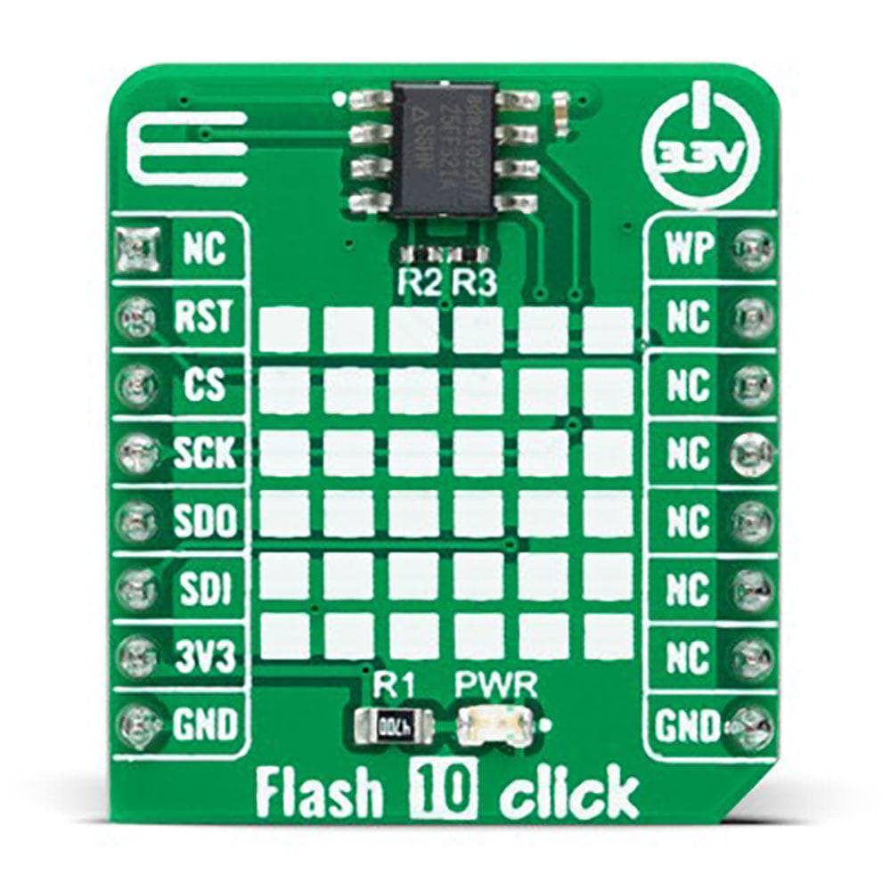
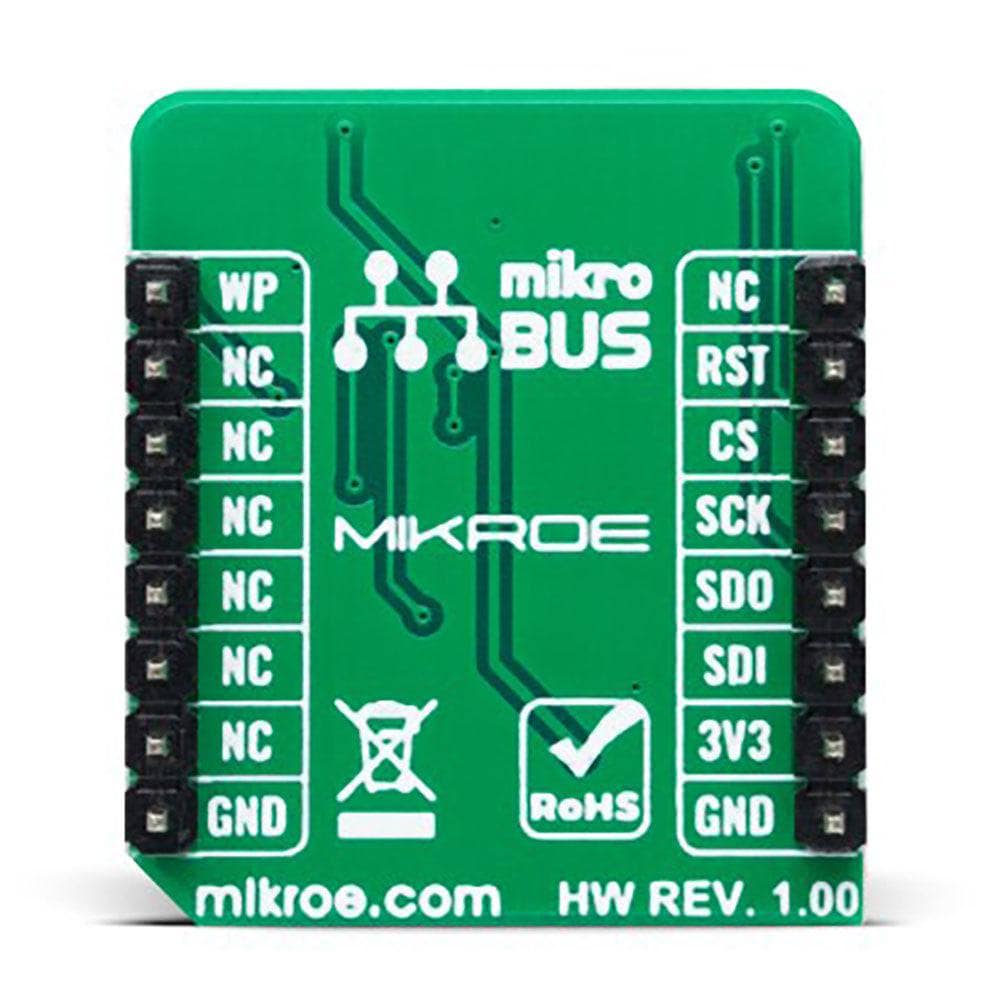
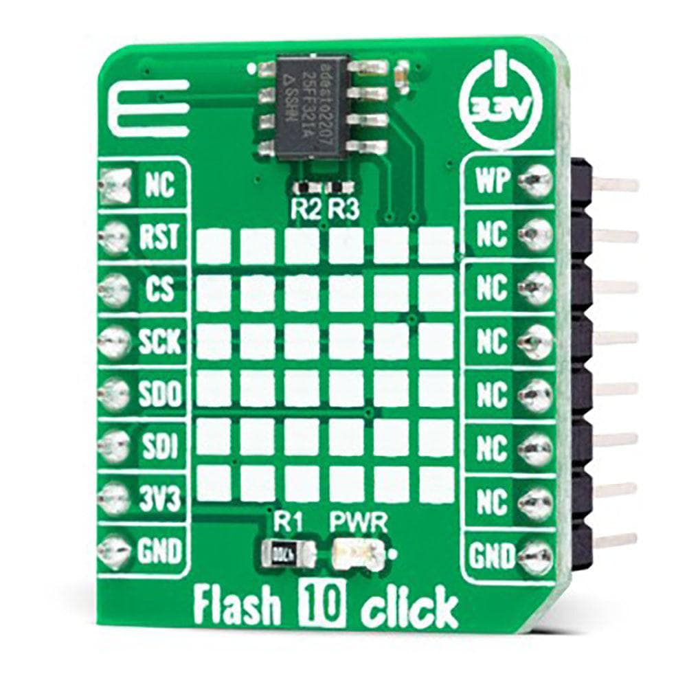
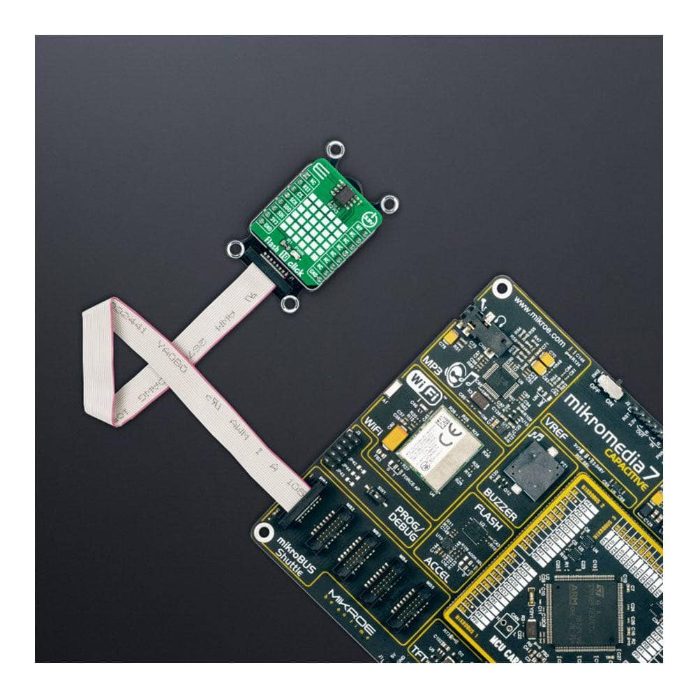
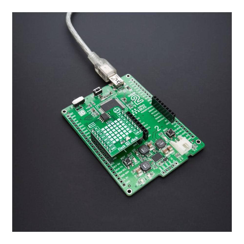
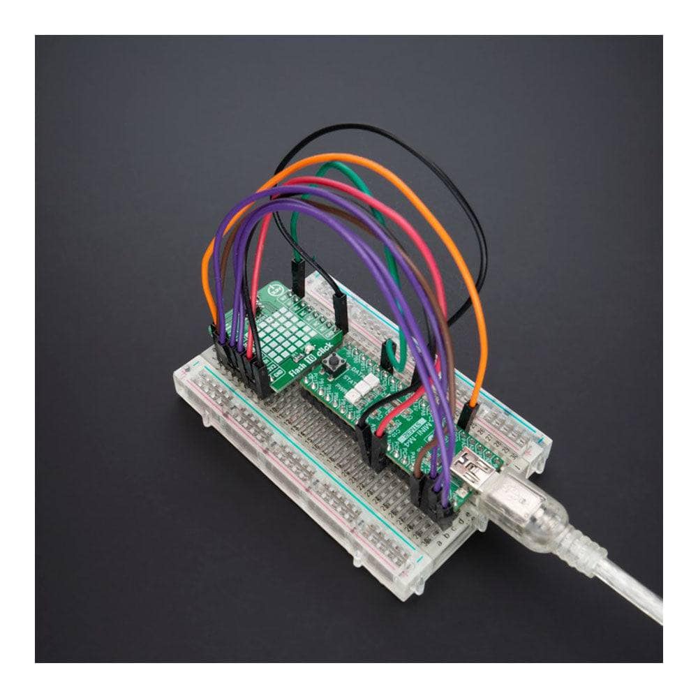
The Flash 10 Click Board™ is a compact add-on board representing a highly reliable memory solution. This board features the AT25FF321A, an SPI configurable 32Mbit (2Mx16) serial Flash memory solution from Dialog Semiconductor. The AT25FF321A is an ideal solution for systems in which program code is shadowed from Flash memory into embedded or external RAM (code shadow) for execution and where small amounts of data are stored and updated locally in the Flash memory. It has a flexible and optimized erase architecture for code and data storage applications, non-volatile protection, and four specialized 128-byte OTP security registers to store a unique device ID and locked key storage. This memory can withstand many write cycles (minimum 100k) and has a data retention period greater than 20 years. This Click board™ is suitable for storage and data transfer in consumer devices, enterprise systems, and industrial applications.
The Flash 10 Click Board™ is supported by a mikroSDK compliant library, which includes functions that simplify software development. This Click board™ comes as a fully tested product, ready to be used on a system equipped with the mikroBUS™ socket.
Downloads
Das Flash 10 Click Board™ ist eine kompakte Zusatzplatine, die eine äußerst zuverlässige Speicherlösung darstellt. Diese Platine verfügt über das AT25FF321A, eine SPI-konfigurierbare serielle 32-Mbit-Flash-Speicherlösung (2Mx16) von Dialog Semiconductor. Das AT25FF321A ist eine ideale Lösung für Systeme, in denen Programmcode zur Ausführung vom Flash-Speicher in eingebetteten oder externen RAM (Code Shadow) gespiegelt wird und in denen kleine Datenmengen lokal im Flash-Speicher gespeichert und aktualisiert werden. Es verfügt über eine flexible und optimierte Löscharchitektur für Code- und Datenspeicheranwendungen, nichtflüchtigen Schutz und vier spezielle 128-Byte-OTP-Sicherheitsregister zum Speichern einer eindeutigen Geräte-ID und eines gesperrten Schlüsselspeichers. Dieser Speicher hält vielen Schreibzyklen stand (mindestens 100 KB) und hat eine Datenaufbewahrungsdauer von mehr als 20 Jahren. Dieses Click Board™ ist für die Speicherung und Datenübertragung in Verbrauchergeräten, Unternehmenssystemen und industriellen Anwendungen geeignet.
Das Flash 10 Click Board™ wird von einer mikroSDK-kompatiblen Bibliothek unterstützt, die Funktionen enthält, die die Softwareentwicklung vereinfachen. Dieses Click Board™ wird als vollständig getestetes Produkt geliefert und ist bereit für den Einsatz auf einem System, das mit der mikroBUS™-Buchse ausgestattet ist.
| General Information | |
|---|---|
Part Number (SKU) |
MIKROE-5289
|
Manufacturer |
|
| Physical and Mechanical | |
Weight |
0.02 kg
|
| Other | |
EAN |
8606027387920
|
Frequently Asked Questions
Have a Question?
Be the first to ask a question about this.