


Mikroelektronika d.o.o.
ADAC 3 Click Board™
ADAC 3 Click Board™
SKU: MIKROE-5198
Verfügbarkeit für Abholungen konnte nicht geladen werden


Key Features
Overview
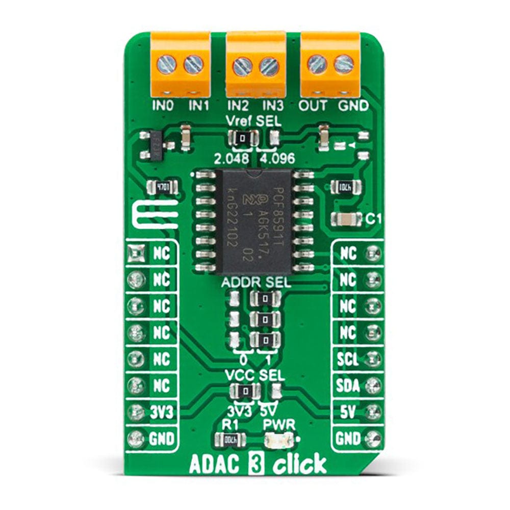
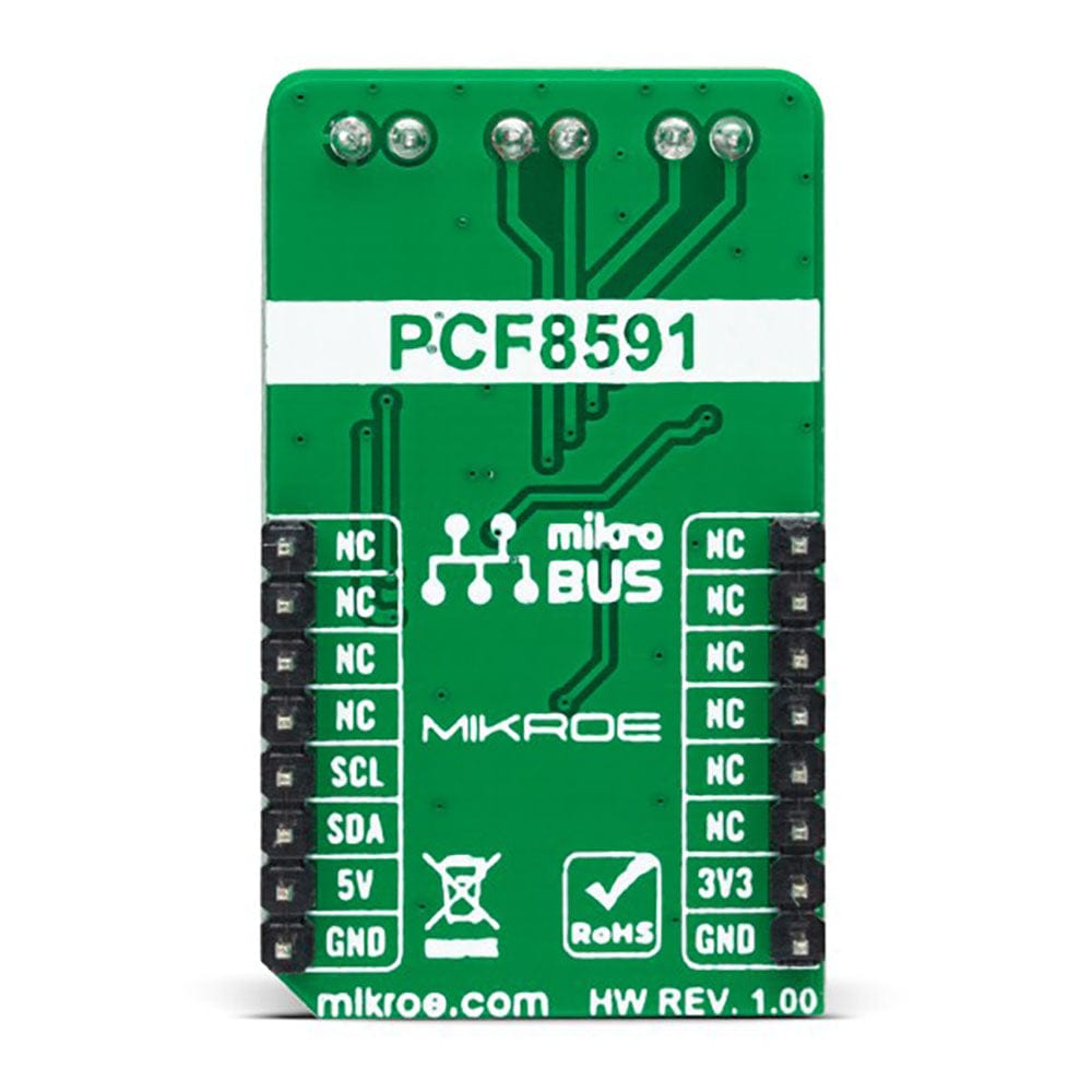
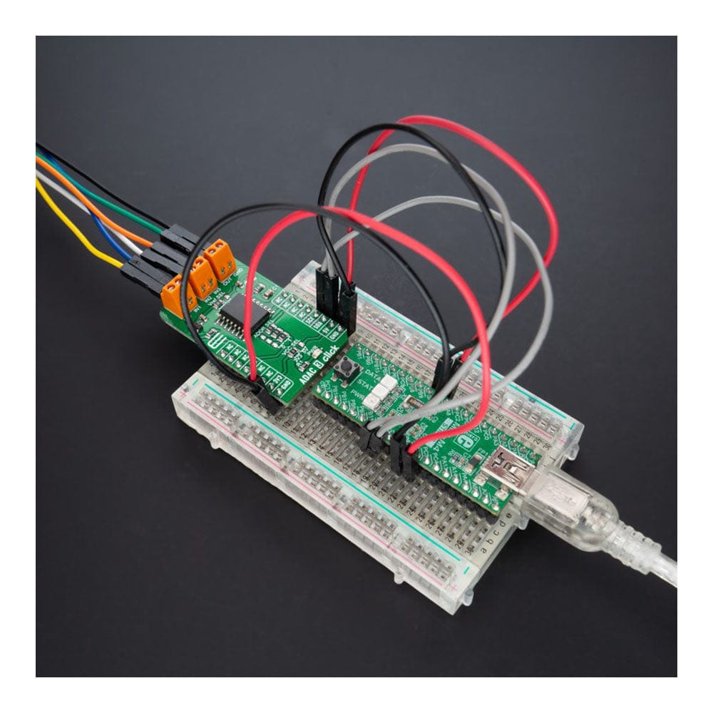
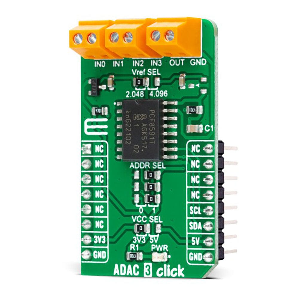
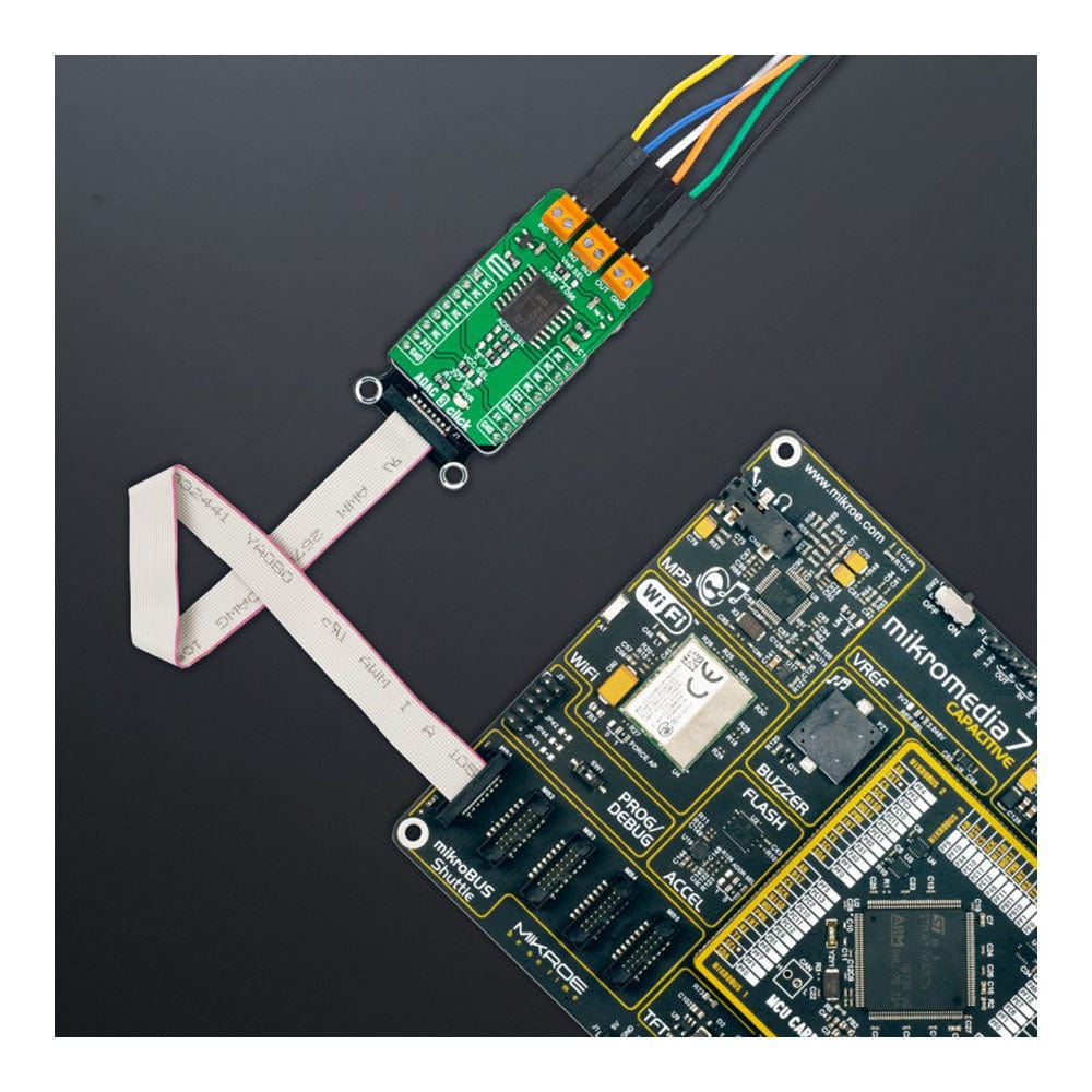
The ADAC 3 Click Board™ is a compact add-on board representing the ADC/DAC combo solution. This board features the PCF8591, a low-power 8-bit CMOS data acquisition device with four analogue inputs, one analogue output, and a serial I2C interface from NXP Semiconductors. The PCF8591 includes analogue input multiplexing, an on-chip track and hold function and 8-bit analogue-to-digital conversion alongside an 8-bit digital-to-analogue conversion. In addition, the user is given the option to select the PCF8591 reference voltage value, choosing between 2,048 and 4,096V. This Click board™ is suitable for various control, monitoring, or measurement applications such as supply monitoring, reference setting, analogue control loops, and more.
The ADAC 3 Click Board™ is supported by a mikroSDK compliant library, which includes functions that simplify software development. This Click board™ comes as a fully tested product, ready to be used on a system equipped with the mikroBUS™ socket.
Downloads
Das ADAC 3 Click Board™ ist eine kompakte Zusatzplatine, die die ADC/DAC-Kombilösung darstellt. Diese Platine verfügt über den PCF8591, ein stromsparendes 8-Bit-CMOS-Datenerfassungsgerät mit vier analogen Eingängen, einem analogen Ausgang und einer seriellen I2C-Schnittstelle von NXP Semiconductors. Der PCF8591 umfasst analoges Eingangsmultiplexing, eine integrierte Track-and-Hold-Funktion und 8-Bit-Analog-Digital-Konvertierung neben einer 8-Bit-Digital-Analog-Konvertierung. Darüber hinaus hat der Benutzer die Möglichkeit, den Referenzspannungswert des PCF8591 auszuwählen und zwischen 2.048 und 4.096 V zu wählen. Dieses Click Board™ ist für verschiedene Steuerungs-, Überwachungs- oder Messanwendungen wie Versorgungsüberwachung, Referenzeinstellung, analoge Regelkreise und mehr geeignet.
Das ADAC 3 Click Board™ wird von einer mikroSDK-kompatiblen Bibliothek unterstützt, die Funktionen enthält, die die Softwareentwicklung vereinfachen. Dieses Click Board™ wird als vollständig getestetes Produkt geliefert und ist bereit für den Einsatz auf einem System, das mit der mikroBUS™-Buchse ausgestattet ist.
| General Information | |
|---|---|
Part Number (SKU) |
MIKROE-5198
|
Manufacturer |
|
| Physical and Mechanical | |
Weight |
0.02 kg
|
| Other | |
EAN |
8606027388330
|
Frequently Asked Questions
Have a Question?
Be the first to ask a question about this.