


Mikroelektronika d.o.o.
Flash 5 Click-Platine
Flash 5 Click-Platine
SKU: MIKROE-3780
Verfügbarkeit für Abholungen konnte nicht geladen werden


Overview
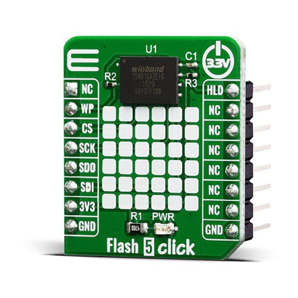
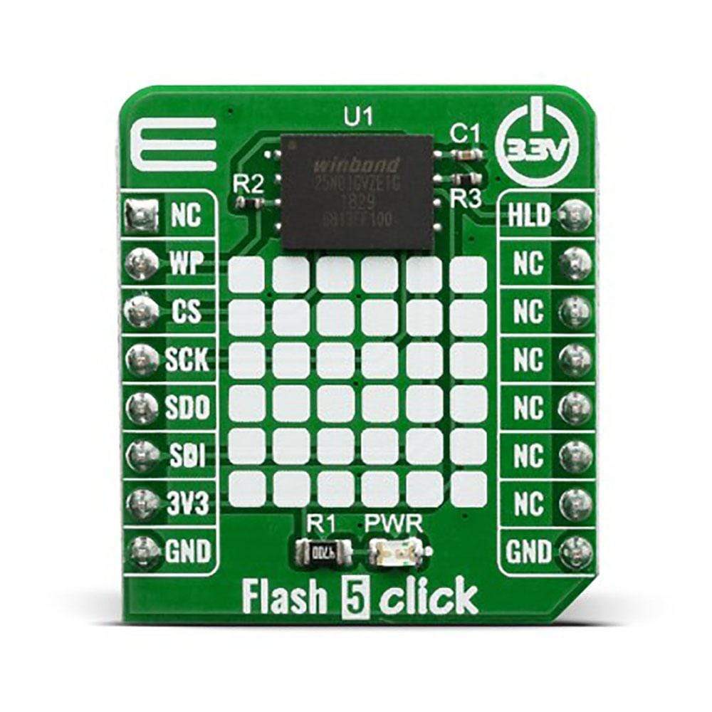
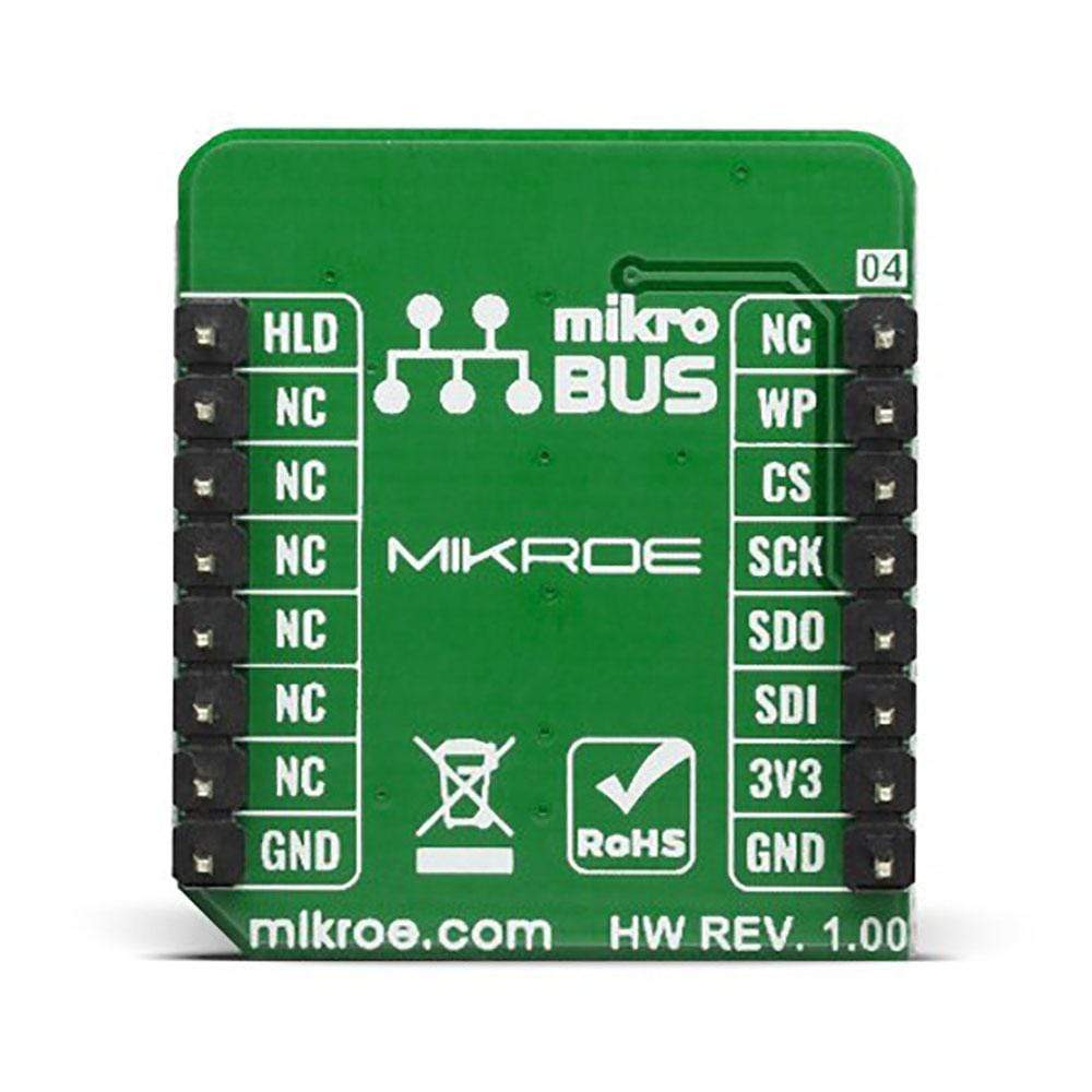
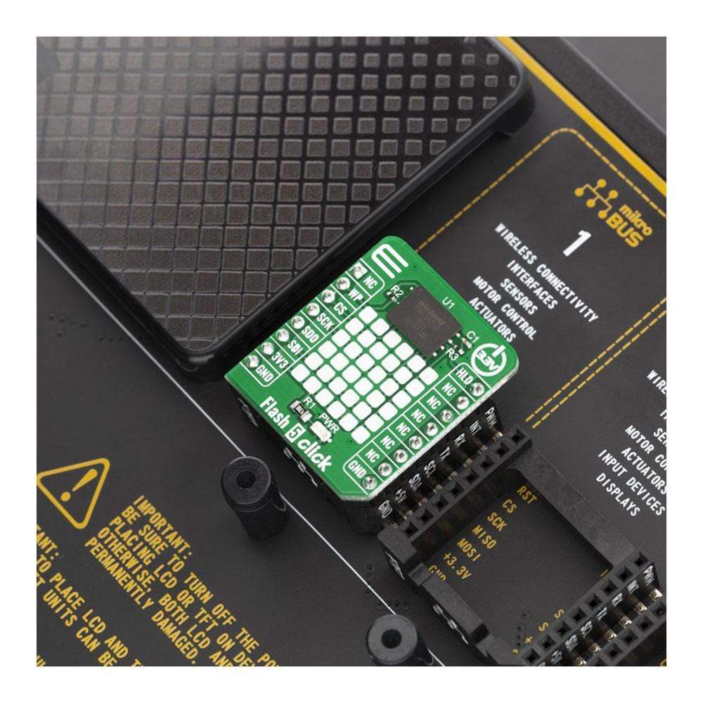
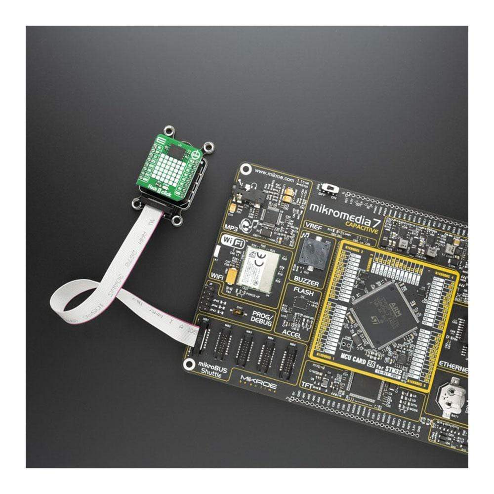
The Flash 5 Click Board™ is a perfect solution for the mass storage option in various embedded applications. It features the W25N01GVZEIG/IT (1G-bit) Serial SLC NAND Flash Memory from Winbond which provides a storage solution for systems with limited space, pins and power. The W25N SpiFlash family incorporates the popular SPI interface and the traditional large NAND non-volatile memory space. They are ideal for code shadowing to RAM, executing code directly from Dual/Quad SPI (XIP) and storing voice, text and data.
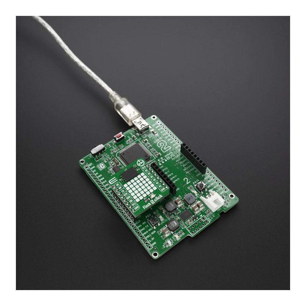
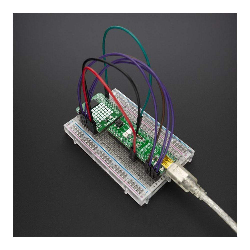
The Flash 5 Click Board™ is supported by a mikroSDK compliant library, which includes functions that simplify software development. This Click Board™ comes as a fully tested product, ready to be used on a system equipped with the mikroBUS™ socket.
Downloads
Das Flash 5 Click Board™ ist eine perfekte Lösung für die Massenspeicheroption in verschiedenen eingebetteten Anwendungen. Es verfügt über den seriellen SLC NAND-Flash-Speicher W25N01GVZEIG/IT (1 GB) von Winbond, der eine Speicherlösung für Systeme mit begrenztem Platz, begrenzten Pins und begrenzter Leistung bietet. Die W25N SpiFlash-Familie umfasst die beliebte SPI-Schnittstelle und den herkömmlichen großen nichtflüchtigen NAND-Speicherplatz. Sie sind ideal für Code-Shadowing in RAM, die Ausführung von Code direkt von Dual/Quad SPI (XIP) und die Speicherung von Sprache, Text und Daten.
Das Flash 5 Click Board™ wird von einer mikroSDK-kompatiblen Bibliothek unterstützt, die Funktionen enthält, die die Softwareentwicklung vereinfachen. Dieses Click Board™ wird als vollständig getestetes Produkt geliefert und ist bereit für den Einsatz auf einem System, das mit der mikroBUS™-Buchse ausgestattet ist.
| General Information | |
|---|---|
Part Number (SKU) |
MIKROE-3780
|
Manufacturer |
|
| Physical and Mechanical | |
Weight |
0.016 kg
|
| Other | |
EAN |
8606018719969
|
Frequently Asked Questions
Have a Question?
Be the first to ask a question about this.