


Mikroelektronika d.o.o.
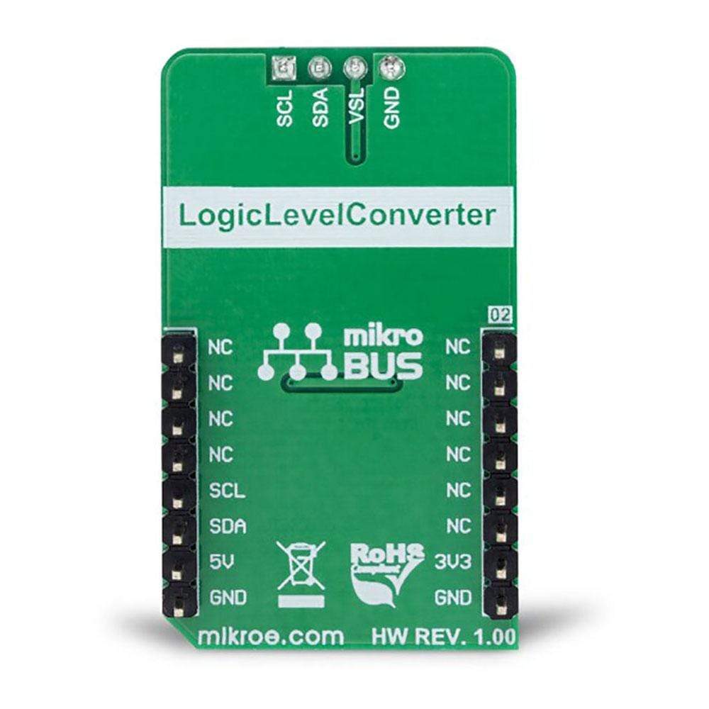
LLC-I2C Click-Platine
LLC-I2C Click-Platine
SKU: MIKROE-3276
Verfügbarkeit für Abholungen konnte nicht geladen werden


Key Features
Overview
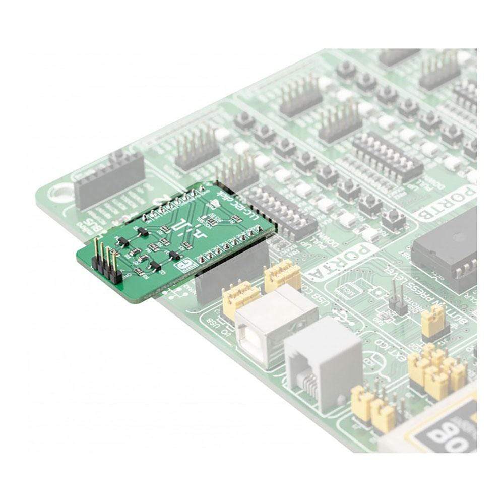
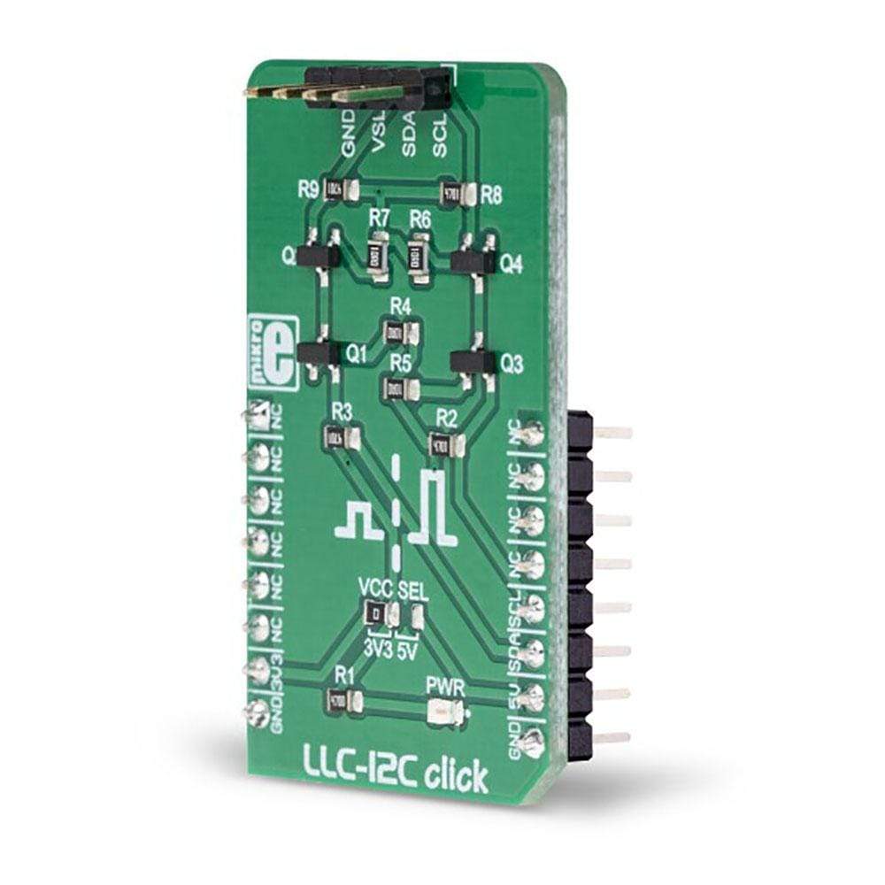
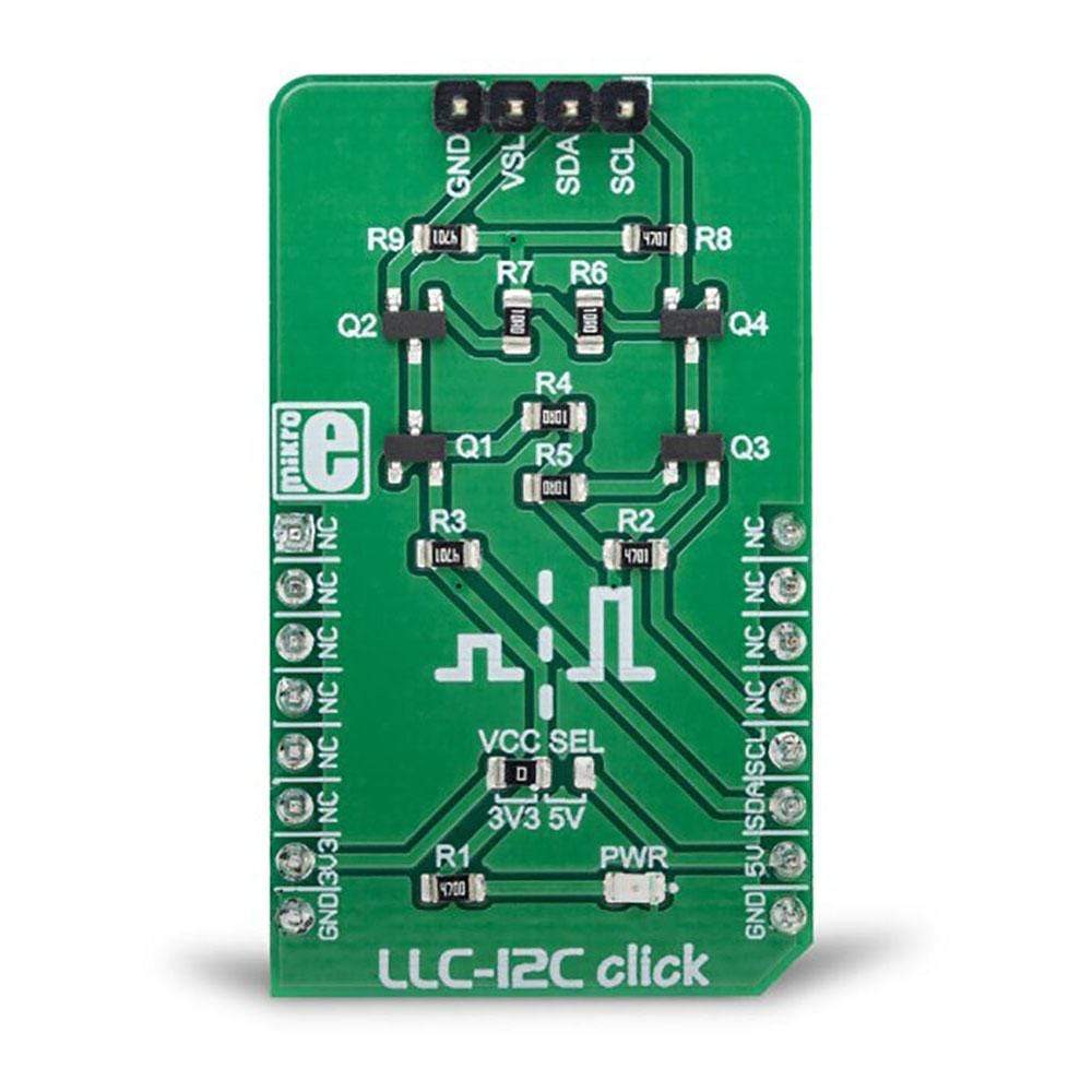
The LLC I2C Click Board™ can be utilized as the level converter for logic signals, which makes it a very useful Click Board™. The topology of this logic level conversion (LLC) circuit is perfectly suited for the bi-directional I2C communication. Although there are some specialised integrated circuits on the market, sometimes it is more convenient to have a simple solution made of just a few passive elements and four MOSFETs. Besides this, MOSFETs can withstand up to 20V across their terminals (12V VGS), and they support far greater currents than typical ICs, making them less likely to fail. The LLC circuitry, also known as the level translator or level shifter, can be used in virtually any application that utilizes the I2C communication protocol and needs matching between the logic voltage levels
Downloads
Das LLC I2C Click Board™ kann als Pegelwandler für Logiksignale verwendet werden, was es zu einem sehr nützlichen Click Board™ macht. Die Topologie dieser Logikpegelumwandlungsschaltung (LLC) ist perfekt für die bidirektionale I2C-Kommunikation geeignet. Obwohl es auf dem Markt einige spezialisierte integrierte Schaltkreise gibt, ist es manchmal bequemer, eine einfache Lösung aus nur wenigen passiven Elementen und vier MOSFETs zu haben. Darüber hinaus können MOSFETs bis zu 20 V über ihre Anschlüsse aushalten (12 V VGS) und sie unterstützen weitaus höhere Ströme als typische ICs, wodurch sie weniger ausfallanfällig sind. Die LLC-Schaltung, auch als Pegelumsetzer oder Pegelschieber bekannt, kann in praktisch jeder Anwendung verwendet werden, die das I2C-Kommunikationsprotokoll verwendet und eine Anpassung der Logikspannungspegel erfordert.
| General Information | |
|---|---|
Part Number (SKU) |
MIKROE-3276
|
Manufacturer |
|
| Physical and Mechanical | |
Weight |
0.019 kg
|
| Other | |
EAN |
8606018714049
|
Frequently Asked Questions
Have a Question?
Be the first to ask a question about this.