Picotest
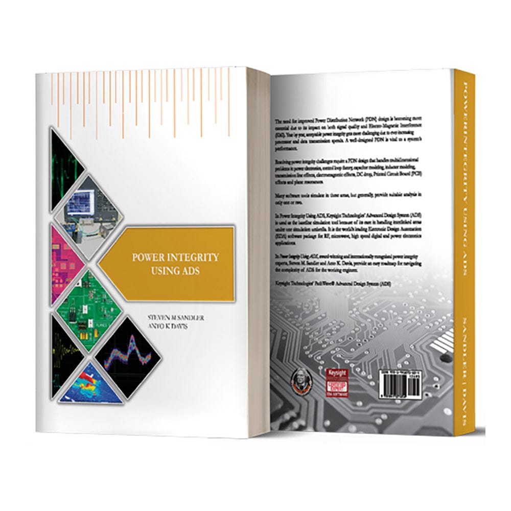
Livre sur l'intégrité de l'alimentation électrique grâce à l'ADS, par Steven Sandler
Livre sur l'intégrité de l'alimentation électrique grâce à l'ADS, par Steven Sandler
Impossible de charger la disponibilité du service de retrait

The need for Power Distribution Network (PDN) simulation is essential due to its impact on power rail compliance, signal integrity, and electro-magnetic interference (EMI). Evolutionary increases in data rates and edge speeds, coincident with decreasing power rail voltages put ever more pressure on power integrity and system engineers to maintain optimum system performance.
Power integrity assurance requires end-to-end simulation including analog and power electronics, as well as, power-aware signal integrity simulation. This also includes details, such as control loop assessment, capacitor and inductor modeling, and DC IR drop including remote sense lines and Printed Circuit Board (PCB) effects.
Keysight Technologies' Pathwave Advanced Design System (ADS), the world's leading Electronic Design Automation (EDA) software package, addresses analog, RF, microwave, high speed digital and power electronics applications, including PCB effects, in a single simulation environment.
Pathwave ADS provides this much needed end-to-end capability including large signal, non-linear Harmonic Balance (HB) simulation. The ADS Harmonic Balance simulator provides ultra-fast time domain and spectral content of switching power supply waveforms and power rail noise without the long simulation times or convergence issues typically associated with transient simulation.
In "Power Integrity Using ADS", award-winning, internationally recognized power integrity guru, and Keysight Certified EDA expert, Steven M. Sandler and Anto K. Davis, share their simulation experience and workspaces to provide a quick and easy guide to best Power Integrity design practices and simulation techniques.
Chapter 1 – An Introduction to ADS
Keysight Technologies' PathWave® Advanced Design System ('ADS') provides a modular simulator environment for practical power integrity studies. This chapter is for those who are not familiar with ADS to get started on the basics. It contains only the basic features necessary for power integrity analysis used in this book. Sample Workspaces are provided.
WORKSPACE DOWNLOAD
| Chapter 2 |
This simulation workspace utilizes schematic driven time domain simulations to design low noise power delivery networks (PDN). The design starts with a simple model of a power delivery network to verify the expected natural step response, forced sinusoidal and square wave responses. The model complexity is increased to add multiple resonances to represent the voltage regulator module (VRM), the PCB inductance with bulk capacitors, and the ceramic decoupling capacitors. An optimizer is then used to search for the maximum voltage noise or rogue wave excursion that can exist with the multiple resonances and a forced digital load pattern from a real world PDN. |
| Chapter 3 |
The workspace has the following sections:
|
| Chapter 4 |
The Workspace contains two folders - "01_InductorModeling" and "02_FerriteBeadsModeling." Both the inductor and ferrite bead models use measured data to obtain the parameters. Sample measured data is available inside the folders "...\AEM_FERRITE_BEADS_wrkndatanInductorMeasuredDatan" and "...\AEM_FERRITE_BEADS_wrkndatanFerriteBeadsMeasuredDatan" Refer to [5, chapter7] for high-fidelity DC biased measurements. The ADS Optimizer is used to tunethe model parameters. A component (inductor or ferrite bead) model can be createdwith its measurement data and the procedure is explained in this chapter. |
| Chapter 5 |
The workspace follows along with the examples in the video and has the following sections:
|
| Chapter 6 & 7 |
This workspace is used by Chapter 6 and Chapter 7. The state space models explained in this workspace are based on measurement results. The power integrity eco-system can be built with the measurement based models by including the PCB layout effects. The Workspace contains the following topics,
|
| Chapter 8 |
This workspace is used by Chapter 9 and Chapter 8. The decoupling capacitor optimizations explained in this workspace are required to obtain a flat impedance profile which is essential for power integrity. The Workspace contains the following topics,
|
| Appendix A |
This Workspace studies various cases of anti-resonant peak formation when two capacitors are connected in parallel. It has the following sections:
|
| Appendix B |
The workspace contains one schematic for studying the effect of ground loop on 2-port shunt-through impedance measurements and how the common mode transformer breaks this loop. The transformer coupling coefficient T=1 breaks the ground loop. The condition T=0 is equivalent to NOT having a transformer in the loop. The Zg is the impedance of the ground loop. The IEC safety standard allows you to have a maximum of 50? in the ground loop which is utilized by some VNAs to break the ground loop. However, this is less effective than having a ground loop breaking common mode transformer or a solid state ground loop breaker. The Zg can be 1nH+0.1m?(represents a small impedance) or 1nH+50m?(allowed maximum impedance through IEC standards). The 1nH represents that the two ports of the VNAs are physically separated and will have a small inductance of the connection. |
| Appendix C |
This Workspace explains with example what the die/chip sees as impedance looking into the PDN. This impedance is not same as the transfer impedance between VRM and the die/chip. The 2-port shunt-through impedance configuration is used to measure ultra-low impedance(m?s and lower) in power integrity measurements. Its connection geometry is such that both the ports are connected to the same point. The differences between the different type of port connections are explained with examples in this Workspace. |
| Downloads |
Livre sur l'intégrité de l'alimentation électrique grâce à l'ADS, par Steven Sandler
Frequently Asked Questions
Have a Question?
Be the first to ask a question about this.

