

Mikroelektronika d.o.o.
Carte à clic pour pilote de pont en H
Carte à clic pour pilote de pont en H
SKU: MIKROE-4696
Impossible de charger la disponibilité du service de retrait


Overview
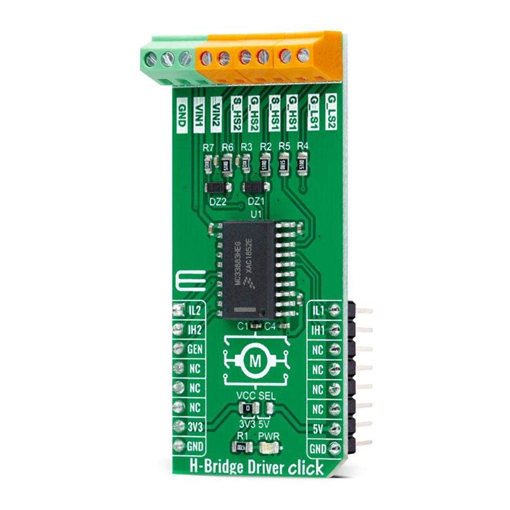
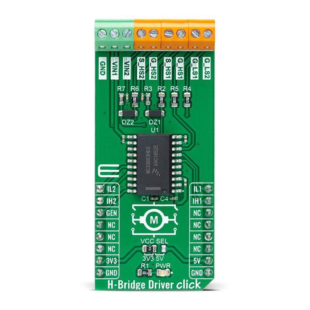
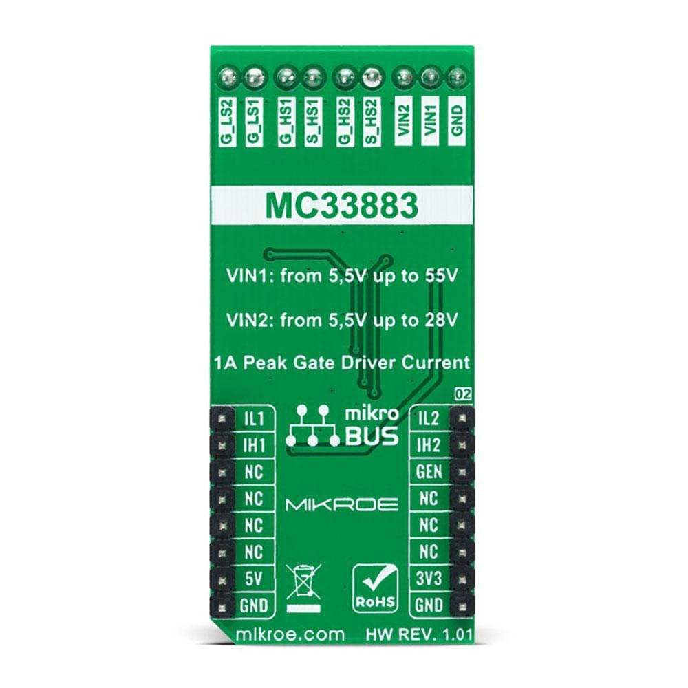
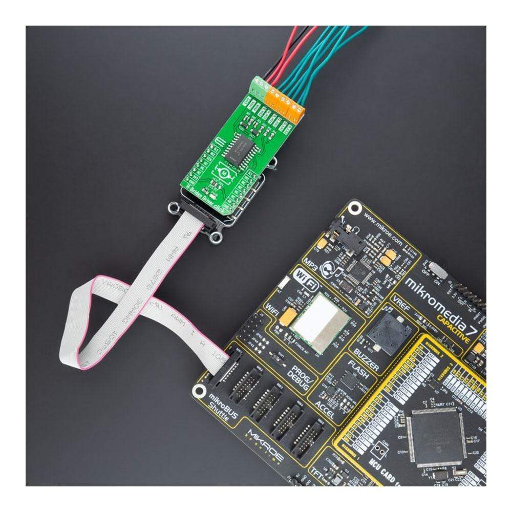
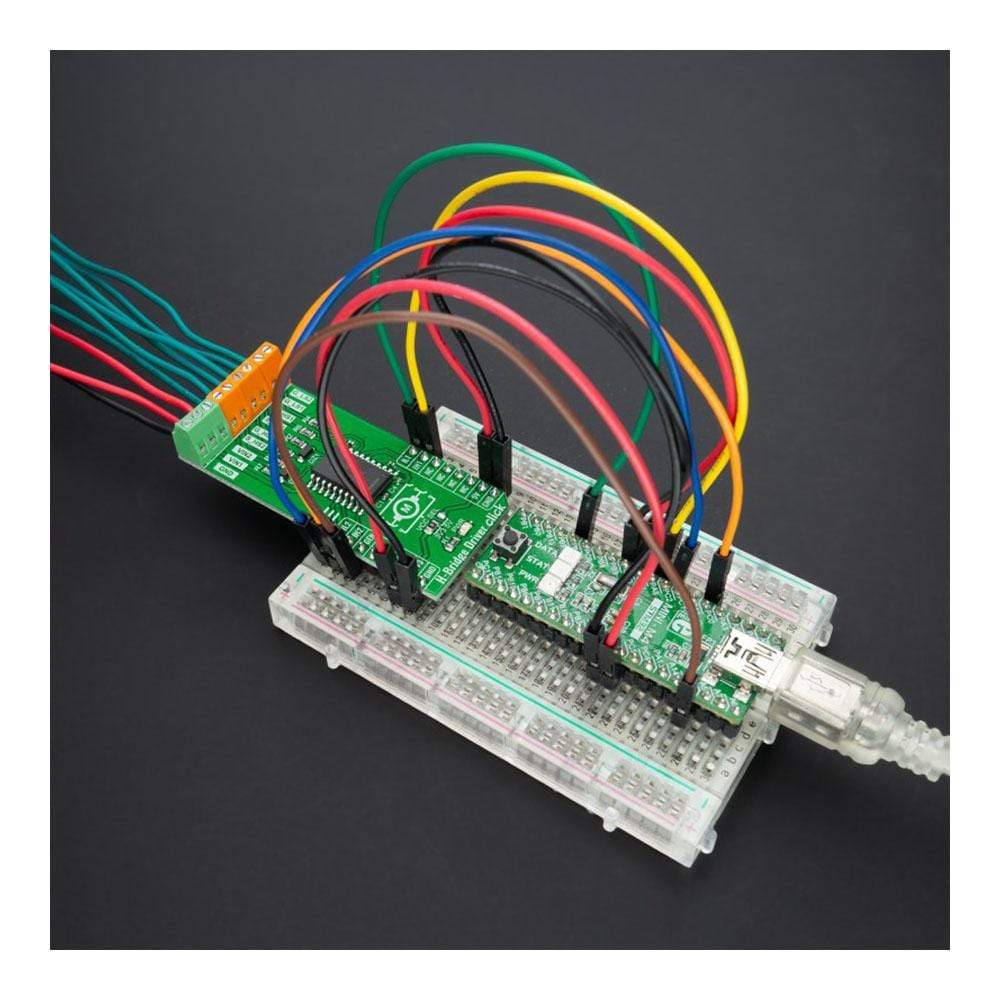
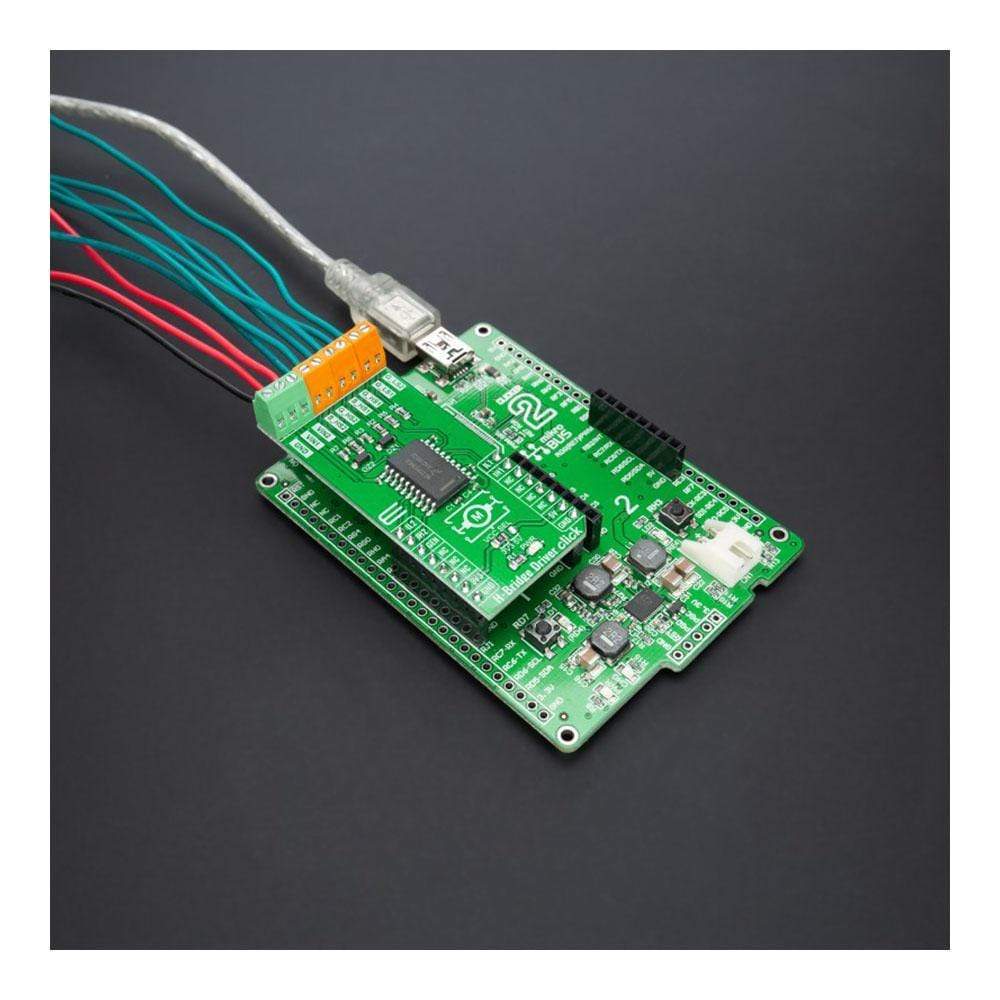
The H-Bridge Driver Click Board™ is a compact add-on board that contains an H-bridge gate driver, also known as a full-bridge pre-driver. This board features the MC33883, an H-Bridge gate driver with an integrated charge pump and independent high and low side gate drive channels from NXP Semiconductors. The gate driver channels are independently controlled by four separate input pins, allowing the device to be optionally configured as two independent high side gate drivers and two independent low side gate drivers. Gate driver outputs can source and sink up to 1.0A peak current pulses, permitting large gate-charge MOSFETs to be driven and/or high pulse-width modulation (PWM) frequencies to be utilized.
The H-Bridge Driver Click Board™ is suitable for automotive engine applications (electric pumps), energy storage systems (ESS), uninterruptible power supply (UPS), and more.
Downloads
La carte Click Board™ H-Bridge Driver est une carte complémentaire compacte qui contient un pilote de grille en pont en H, également connu sous le nom de pré-pilote en pont complet. Cette carte comprend le MC33883, un pilote de grille en pont en H avec une pompe de charge intégrée et des canaux de commande de grille indépendants côté haut et côté bas de NXP Semiconductors. Les canaux de commande de grille sont contrôlés indépendamment par quatre broches d'entrée distinctes, ce qui permet de configurer en option le dispositif comme deux pilotes de grille côté haut indépendants et deux pilotes de grille côté bas indépendants. Les sorties du pilote de grille peuvent générer et absorber des impulsions de courant de crête allant jusqu'à 1,0 A, ce qui permet de piloter des MOSFET à charge de grille importante et/ou d'utiliser des fréquences de modulation de largeur d'impulsion (PWM) élevées.
Le H-Bridge Driver Click Board™ convient aux applications de moteurs automobiles (pompes électriques), aux systèmes de stockage d'énergie (ESS), aux alimentations sans interruption (UPS) et bien plus encore.
| General Information | |
|---|---|
Part Number (SKU) |
MIKROE-4696
|
Manufacturer |
|
| Physical and Mechanical | |
Weight |
0.02 kg
|
| Other | |
EAN |
8606027383182
|
Frequently Asked Questions
Have a Question?
Be the first to ask a question about this.