


Mikroelektronika d.o.o.
Carte à clic DAC 6
Carte à clic DAC 6
Impossible de charger la disponibilité du service de retrait
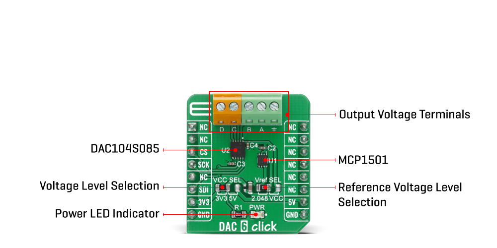
Le Carte Click Board DAC 6™ est une carte complémentaire compacte qui contient un convertisseur numérique-analogique à sortie de tension polyvalent et complet. Cette carte comprend le DAC104S085, 10 bits, micro-alimentation, un convertisseur numérique-analogique quadruple avec sortie rail-à-rail, de Texas Instruments. Il utilise l'interface série SPI à 3 fils pour la communication, qui fonctionne à des fréquences d'horloge allant jusqu'à 40 MHz. En outre, le DAC 6 Click dispose également du MCP1501 intégré, qui est une référence de tension tamponnée de haute précision de 2,048 V. De nombreuses fonctionnalités telles qu'une faible consommation, une sortie de tension rail-à-rail, une sortie à quatre canaux, etc., en font un excellent choix pour une utilisation dans des équipements alimentés par batterie, un réglage numérique du gain et du décalage, des sources de tension et de courant programmables, et bien d'autres encore.
Le Carte à clic DAC 6™ est pris en charge par une bibliothèque compatible mikroSDK, qui comprend des fonctions qui simplifient le développement logiciel. Cette Click Board™ est un produit entièrement testé, prêt à être utilisé sur un système équipé du socket mikroBUS™.


How Does The DAC 6 Click Board™?
The DAC 6 Click Board™ is based on the DAC104S085, 10-bit resolution micro-power QUAD digital-to-analog converter with rail-to-rail output, from Texas Instruments. The DAC104S085 is manufactured on a CMOS process with an architecture that consists of switches and resistor strings that are followed by an output buffer. The reference voltage is applied at the VREFIN pin and is shared by all four DAC outputs (A, B, C, and D). This string consists of 1024 equal valued resistors with a switch at each junction of two resistors, plus a switch to the ground. The code loaded into the DAC register determines which switch is closed, connecting the proper node to the amplifier.
The voltage reference pin of the DAC104S085 is not buffered, and because of that, it is recommended to drive the VREFIN pin by a voltage source with a low output impedance. This is accomplished using the MCP1501, a low drift bandgap-based voltage reference from Microchip capable of sinking and sourcing 20mA of current. The bandgap uses chopper-based amplifiers, effectively reducing the drift to zero. The reference voltage range which can be applied to the VREFIN pin is 1V to VCC (in this case 2.048V), providing the widest possible output dynamic range with a maximum output current of 11mA per channel.
The DAC 6 Click Board™ communicates with MCU using the 3-Wire SPI serial interface that is compatible with standard SPI, QSPI™, MICROWIRE™ and operates at clock rates up to 40 MHz. To use the full dynamic range of the DAC104S085, it is possible to connect the VREFIN pin to the supply voltage VCC. Because of its low power consumption, a reference source may be used as the reference input or the supply voltage which results in accuracy and stability. The reference voltage level can be selected by positioning the SMD jumper labeled as VREF SEL to an appropriate position, selecting between a value of 2.048V and the supply voltage VCC.
The DAC 6 Click Board™ uses the SPI communication interface with both 3.3V and 5V. The onboard SMD jumper labeled as VCC SEL allows voltage selection for interfacing with both 3.3V and 5V MCUs. More information about the DAC104S085's functionality, electrical specifications, and typical performance can be found in the attached datasheet. However, the Click board™ comes equipped with a library that contains easy to use functions and a usage example that may be used as a reference for the development.
SPECIFICATIONS
| Type | DAC |
| Applications | Can be used in battery-operated equipment, digital gain and offset adjustment, programmable voltage and current sources, and many more. |
| On-board modules | The DAC 6 Click Board™ is based on the DAC104S085, 10-bit resolution micro-power QUAD digital-to-analog converter with rail-to-rail output, from Texas Instruments. |
| Key Features | Low power consumption, rail-to-rail voltage output, accuracy, stability, small package, and more. |
| Interface | SPI |
| Compatibility | mikroBUS |
| Click board size | S (28.6 x 25.4 mm) |
| Input Voltage | 3.3V or 5V |
PINOUT DIAGRAM
This table shows how the pinout on the DAC 6 Click Board™ corresponds to the pinout on the mikroBUS™ socket (the latter shown in the two middle columns).
| Notes | Pin | Pin | Notes | ||||
|---|---|---|---|---|---|---|---|
| NC | 1 | AN | PWM | 16 | NC | ||
| NC | 2 | RST | INT | 15 | NC | ||
| SPI Chip Select | CS | 3 | CS | RX | 14 | NC | |
| SPI Clock | SCK | 4 | SCK | TX | 13 | NC | |
| NC | 5 | MISO | SCL | 12 | NC | ||
| SPI Data IN | SDI | 6 | MOSI | SDA | 11 | NC | |
| Power Supply | 3.3V | 7 | 3.3V | 5V | 10 | 5V | Power Supply |
| Ground | GND | 8 | GND | GND | 9 | GND | Ground |
ONBOARD SETTINGS AND INDICATORS
| Label | Name | Default | Description |
|---|---|---|---|
| LD1 | PWR | - | Power LED Indicator |
| JP1 | VCC SEL | Left | Power Supply Voltage Selection 3V3/5V: Left position 3V3, Right position 5V |
| JP2 | VREF SEL | Left | Reference Voltage Level Selection: Left position 2.048V, Right position VCC |
DAC 6 CLICK ELECTRICAL SPECIFICATIONS
| Description | Min | Typ | Max | Unit |
|---|---|---|---|---|
| Supply Voltage VCC | -0.3 | - | 6.5 | V |
| Reference Voltage VREF | 1 | - | VCC | V |
| Maximum Output Current | - | - | 11 | mA |
| SPI Clock Frequency | - | - | 40 | V |
| Operating Temperature Range | -40 | - | +125 | V |
Software Support
We provide a library for the DAC 6 Click Board™ on our LibStock page, as well as a demo application (example), developed using MikroElektronika compilers. The demo can run on all the main MikroElektronika development boards.
Library Description
This library holds functions that can be used to write data to the device's input shift register, or to set operation mode output channel and level.
Key Functions
void dac6_write_data ( uint16_t wr_data )- Sends 16-bit data to the device's input shift register.void dac6_set_output ( uint8_t chan, uint8_t op_mod, uint16_t set_out )- Function is used to set operation mode output channel and level.
Example Description
The application is composed of three sections :
- System Initialization - Initializes GPIO, SPI and LOG structures.
- Application Initialization - Initalizes SPI driver.
- Application Task - (code snippet) This example shows capabilities of DAC 6 click by changeing output values from 0 to the maximum output range on all four channels. Output voltage is calculated by using the equation : Vout = Vrefin * (set_out / 4095).
void application_task ( )
{
 for ( n_cnt = 0; n_cnt < 4096; n_cnt += 315 )
 {
 v_out = dac6_set_output ( DAC6_CHANNEL_A,
 DAC6_WRITE_ALL_AND_UPDATE,
 DAC6_V_REF_2048,
 n_cnt );
 FloatToStr( v_out, log_text );
 mikrobus_logWrite( " VOUT ~ ", _LOG_TEXT );
 mikrobus_logWrite( log_text, _LOG_TEXT );
 mikrobus_logWrite( " mV", _LOG_LINE );
 mikrobus_logWrite( "--------------------", _LOG_LINE );
 Delay_ms( 5000 );
 }
 Delay_ms( 5000 );
}
The full application code, and ready to use projects can be found on our LibStock page.
Other mikroE Libraries used in the example:
- SPI
- UART
- Conversions
Additional Notes and Information
Depending on the development board you are using, you may need a USB UART click, USB UART 2 click or RS232 click to connect to your PC, for development systems with no UART to USB interface available on the board. The terminal available in all MikroElektronika compilers, or any other terminal application of your choice, can be used to read the message.
MIKROSDK
The DAC 6 Click Board™ is supported with mikroSDK - MikroElektronika Software Development Kit. To ensure proper operation of mikroSDK compliant Click board™ demo applications, mikroSDK should be downloaded from the LibStock and installed for the compiler you are using.
Carte à clic DAC 6
Frequently Asked Questions
Have a Question?
Be the first to ask a question about this.