


Mikroelektronika d.o.o.
Carte SRAM 2 Click
Carte SRAM 2 Click
SKU: MIKROE-4178
Impossible de charger la disponibilité du service de retrait


Overview
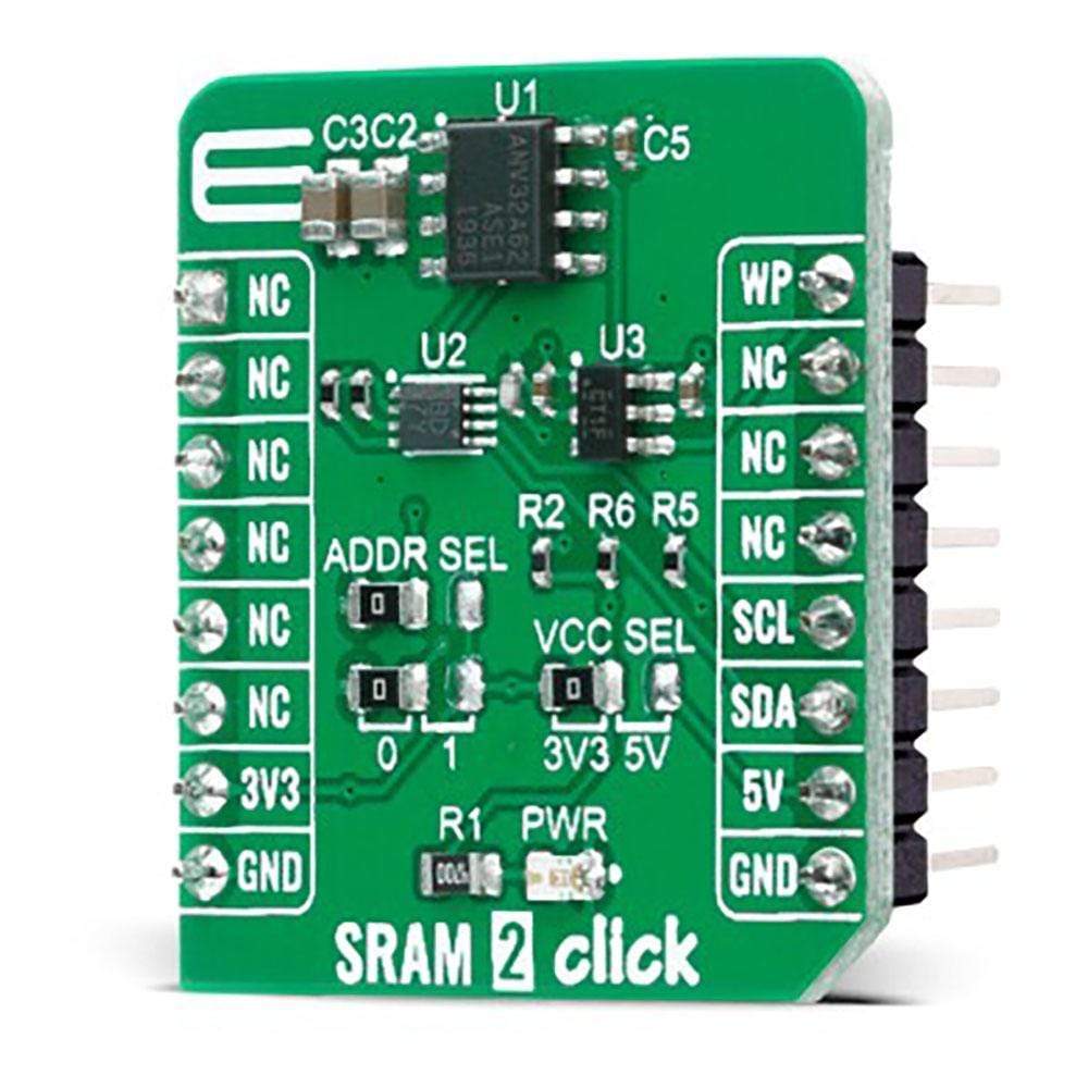
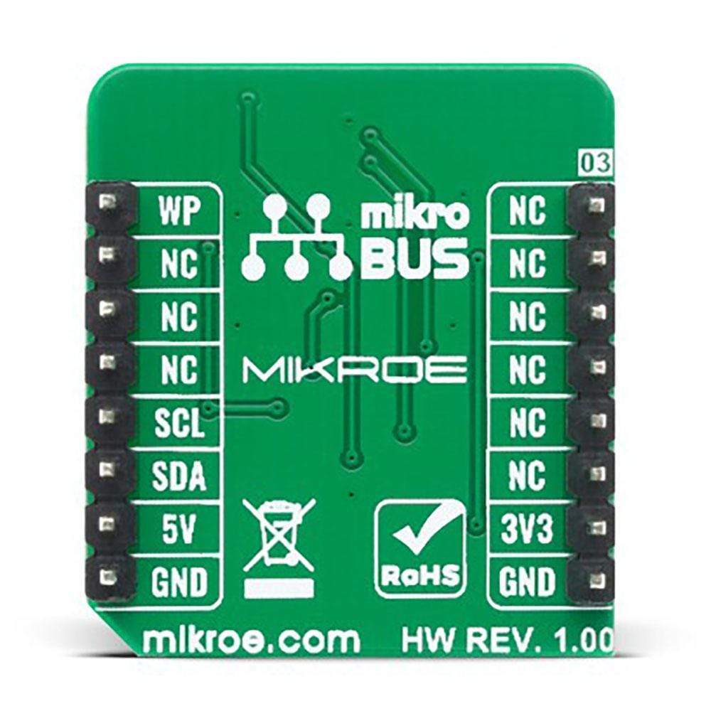
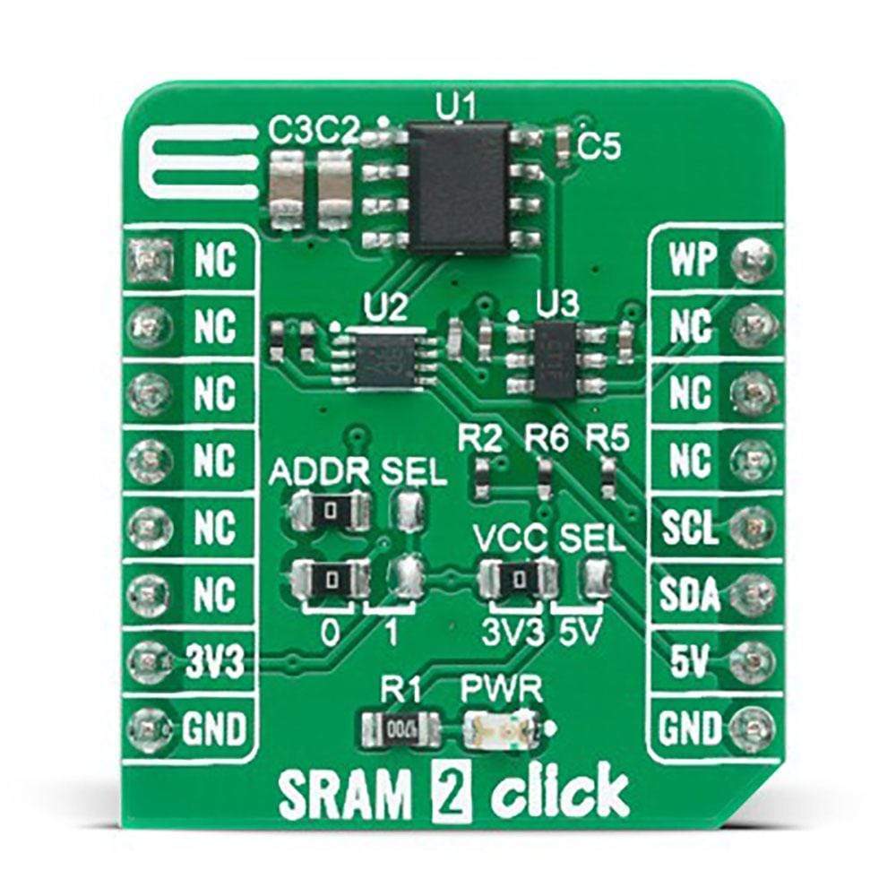
The SRAM 2 Click Board™ is based on ANV32A62A SRAM memory from Anvo-Systems Dresden. It's a 64Kb serial SRAM with a non-volatile SONOS storage element included with each memory cell, organized as 8k words of 8 bits each. Communication is done by an I²C with up to 4 cascadable devices that can share the common bus. The serial nvSRAM provides the access and cycle times, easy to use and unlimited read and write endurance of an SRAM.
The SRAM 2 Click Board™ can be easily used to store drive profiles, configurations and similar data, which are typically stored in a FLASH.
Downloads
La carte SRAM 2 Click Board™ est basée sur la mémoire SRAM ANV32A62A d'Anvo-Systems Dresden. Il s'agit d'une SRAM série de 64 Ko avec un élément de stockage SONOS non volatil inclus avec chaque cellule mémoire, organisé en 8 000 mots de 8 bits chacun. La communication est effectuée par un I²C avec jusqu'à 4 périphériques cascadables pouvant partager le bus commun. La nvSRAM série fournit les temps d'accès et de cycle, la facilité d'utilisation et l'endurance illimitée en lecture et en écriture d'une SRAM.
La carte SRAM 2 Click Board™ peut être facilement utilisée pour stocker des profils de lecteur, des configurations et des données similaires, qui sont généralement stockées dans une mémoire FLASH.
| General Information | |
|---|---|
Part Number (SKU) |
MIKROE-4178
|
Manufacturer |
|
| Physical and Mechanical | |
Weight |
0.016 kg
|
| Other | |
EAN |
8606018717941
|
Frequently Asked Questions
Have a Question?
Be the first to ask a question about this.