


Mikroelektronika d.o.o.
Tableau de clic Flash 5
Tableau de clic Flash 5
SKU: MIKROE-3780
Impossible de charger la disponibilité du service de retrait


Overview
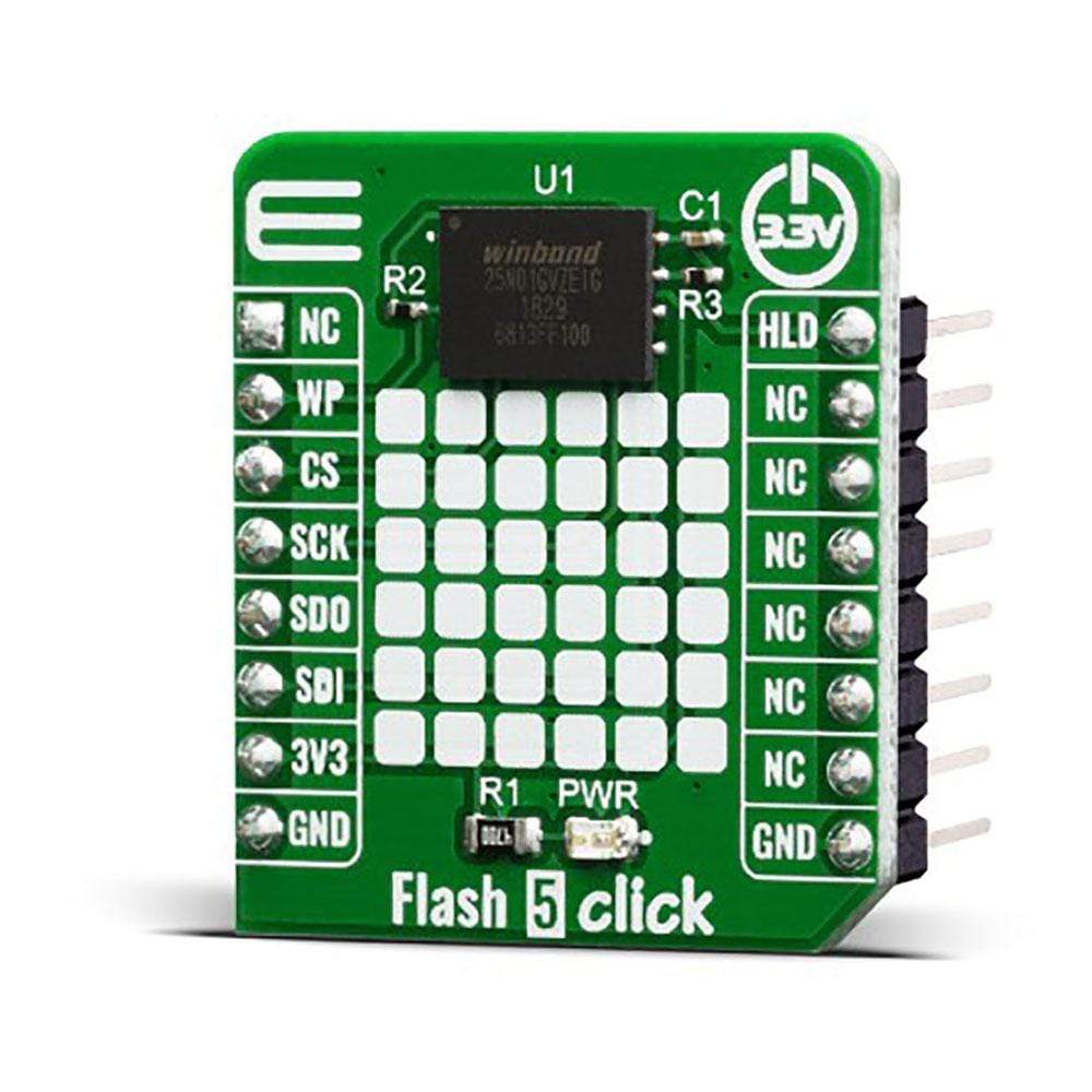
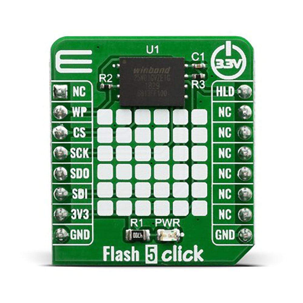
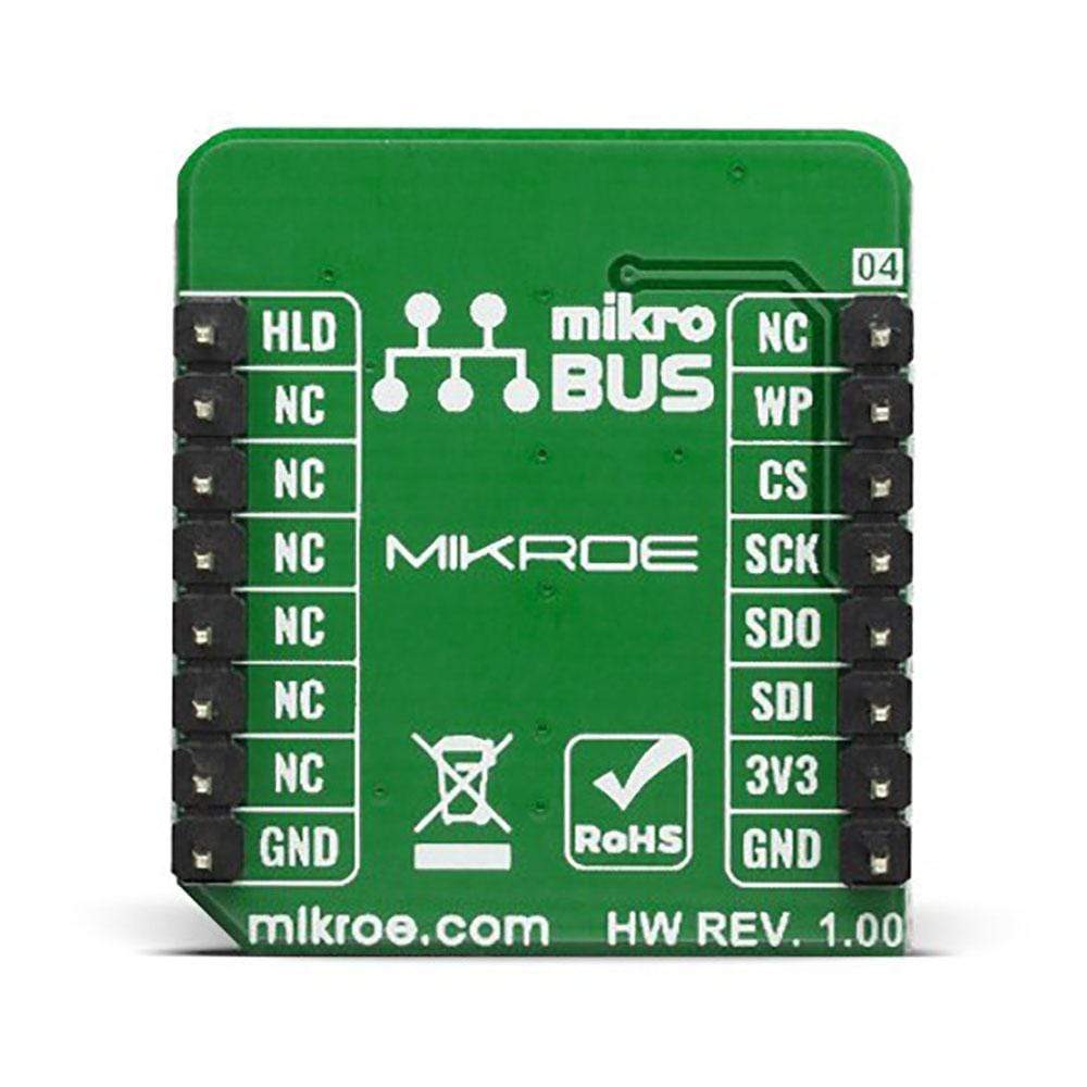
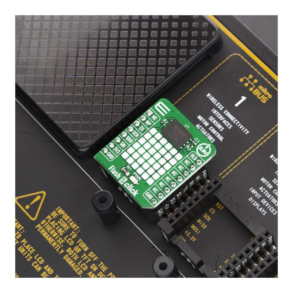
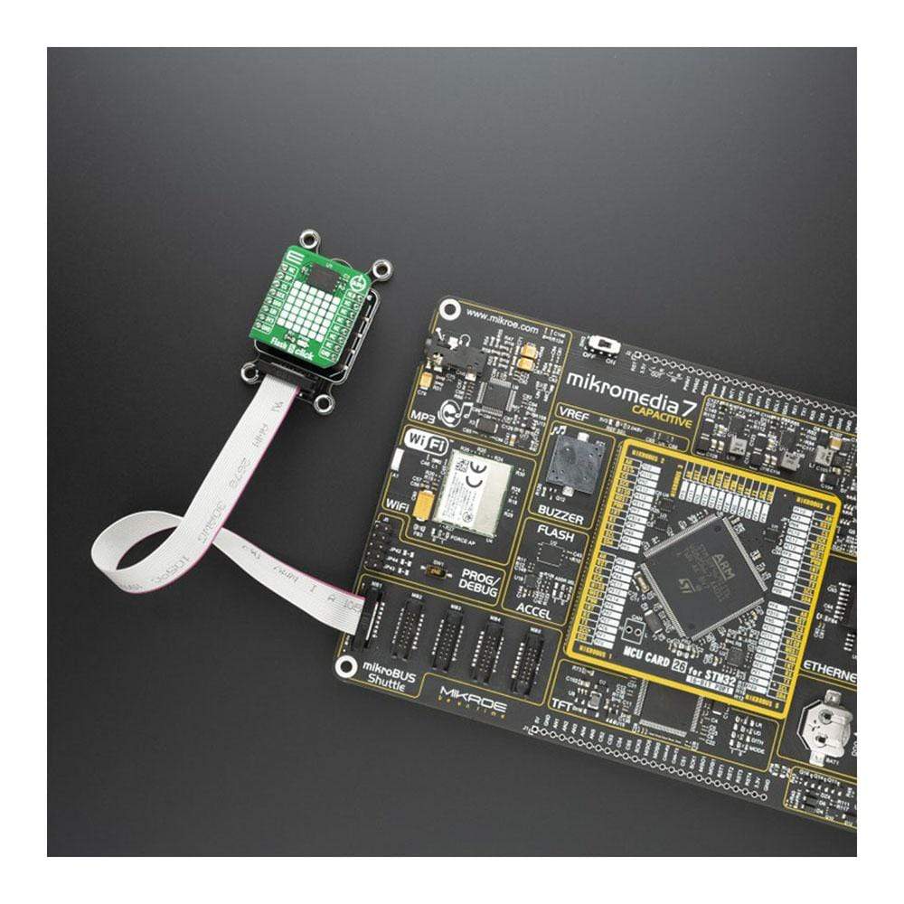
The Flash 5 Click Board™ is a perfect solution for the mass storage option in various embedded applications. It features the W25N01GVZEIG/IT (1G-bit) Serial SLC NAND Flash Memory from Winbond which provides a storage solution for systems with limited space, pins and power. The W25N SpiFlash family incorporates the popular SPI interface and the traditional large NAND non-volatile memory space. They are ideal for code shadowing to RAM, executing code directly from Dual/Quad SPI (XIP) and storing voice, text and data.
The Flash 5 Click Board™ is supported by a mikroSDK compliant library, which includes functions that simplify software development. This Click Board™ comes as a fully tested product, ready to be used on a system equipped with the mikroBUS™ socket.
Downloads
La carte Flash 5 Click Board™ est une solution parfaite pour le stockage de masse dans diverses applications embarquées. Elle est équipée de la mémoire flash NAND SLC série W25N01GVZEIG/IT (1 Go) de Winbond qui offre une solution de stockage pour les systèmes avec un espace, des broches et une puissance limités. La famille SpiFlash W25N intègre l'interface SPI populaire et le grand espace mémoire non volatile NAND traditionnel. Elles sont idéales pour le shadowing de code dans la RAM, l'exécution de code directement à partir de Dual/Quad SPI (XIP) et le stockage de la voix, du texte et des données.
La carte Flash 5 Click Board™ est supportée par une bibliothèque compatible mikroSDK, qui comprend des fonctions qui simplifient le développement logiciel. Cette carte Click Board™ est un produit entièrement testé, prêt à être utilisé sur un système équipé du socket mikroBUS™.
| General Information | |
|---|---|
Part Number (SKU) |
MIKROE-3780
|
Manufacturer |
|
| Physical and Mechanical | |
Weight |
0.016 kg
|
| Other | |
EAN |
8606018719969
|
Frequently Asked Questions
Have a Question?
Be the first to ask a question about this.