


Mikroelektronika d.o.o.
Carte à clic ADC 8
Carte à clic ADC 8
SKU: MIKROE-3394
Impossible de charger la disponibilité du service de retrait


Key Features
Overview
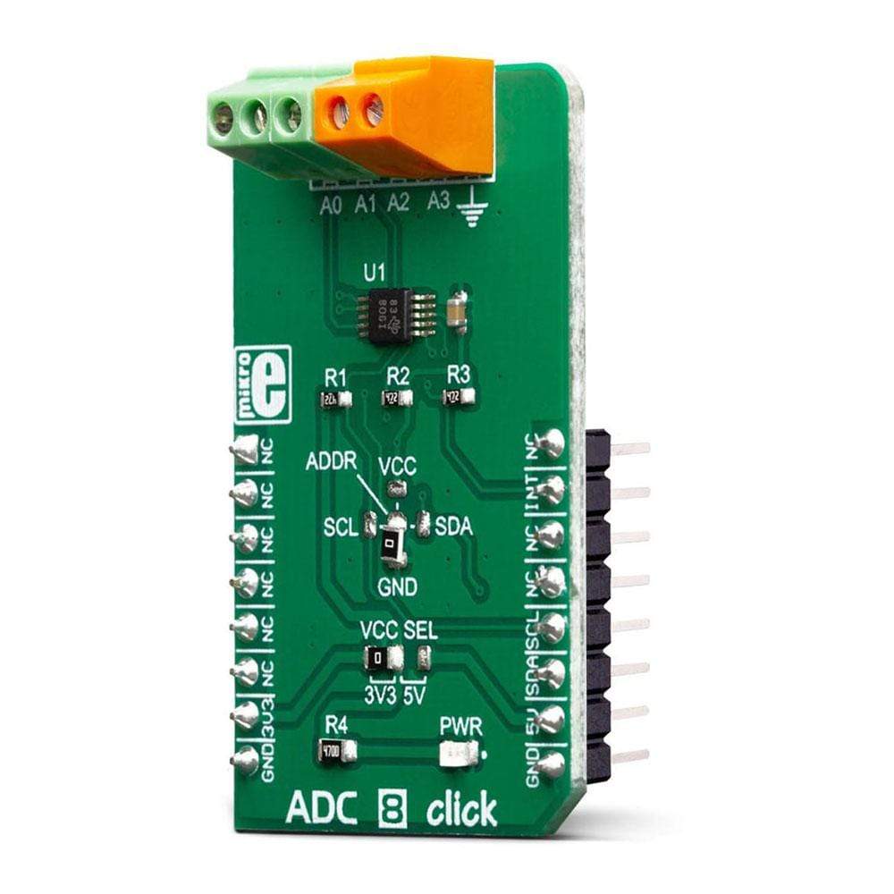
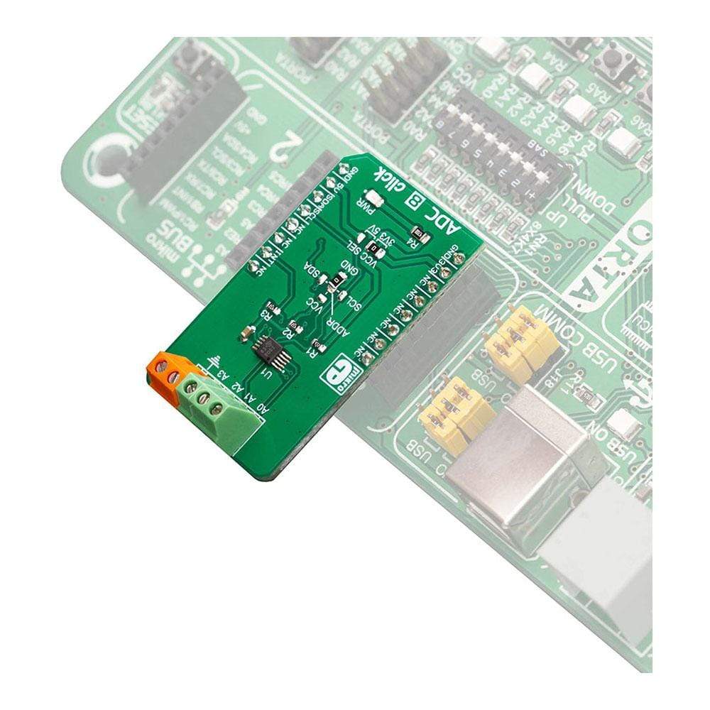
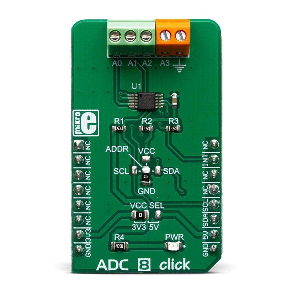
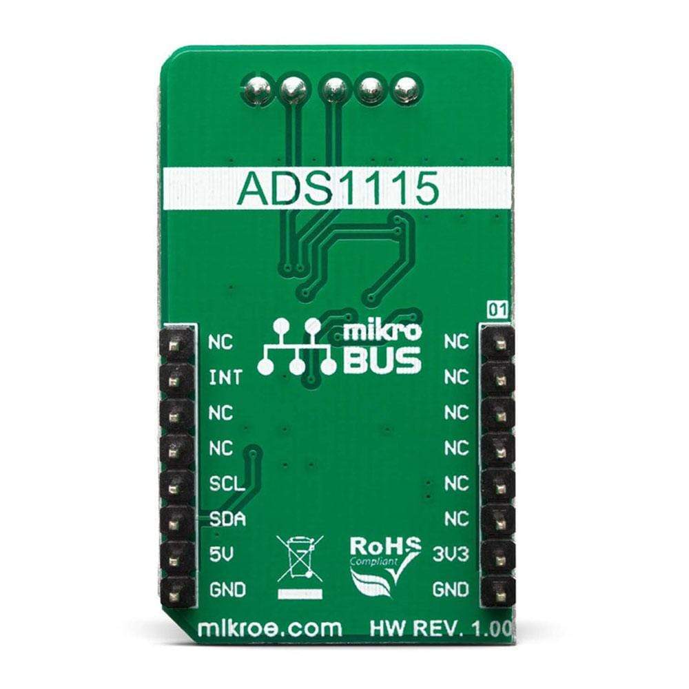
The ADC 8 Click Board™ is a high precision, low-power, 16-bit analogue-to-digital converter (ADC), based around the ADS1115 IC. It is capable of sampling signals on four single-ended or two differential input channels.
Although the ADS1115 cannot use an external reference, it incorporates a low-drift programmable voltage reference, along with the programmable gain amplifier (PGA). This allows for great flexibility in terms of the input signal level: it can sample signals from ±256 mV, up to 6.144 V, allowing a very high precision for a wide range of input signals, making it an excellent choice for various instrumentation applications.
Downloads
L' ADC 8 Click Board™ est un convertisseur analogique-numérique (ADC) 16 bits de haute précision et à faible consommation, basé sur le circuit intégré ADS1115. Il est capable d'échantillonner des signaux sur quatre canaux d'entrée asymétriques ou deux canaux d'entrée différentiels.
Bien que l'ADS1115 ne puisse pas utiliser de référence externe, il intègre une référence de tension programmable à faible dérive, ainsi qu'un amplificateur de gain programmable (PGA). Cela permet une grande flexibilité en termes de niveau de signal d'entrée : il peut échantillonner des signaux de ±256 mV, jusqu'à 6,144 V, ce qui permet une très haute précision pour une large gamme de signaux d'entrée, ce qui en fait un excellent choix pour diverses applications d'instrumentation.
| General Information | |
|---|---|
Part Number (SKU) |
MIKROE-3394
|
Manufacturer |
|
| Physical and Mechanical | |
Weight |
0.02 kg
|
| Other | |
EAN |
8606018714674
|
Frequently Asked Questions
Have a Question?
Be the first to ask a question about this.