


Mikroelektronika d.o.o.
Tableau de clic LLC-SPI
Tableau de clic LLC-SPI
SKU: MIKROE-3298
Impossible de charger la disponibilité du service de retrait


Overview
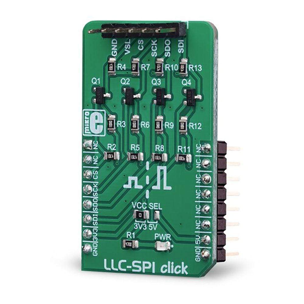
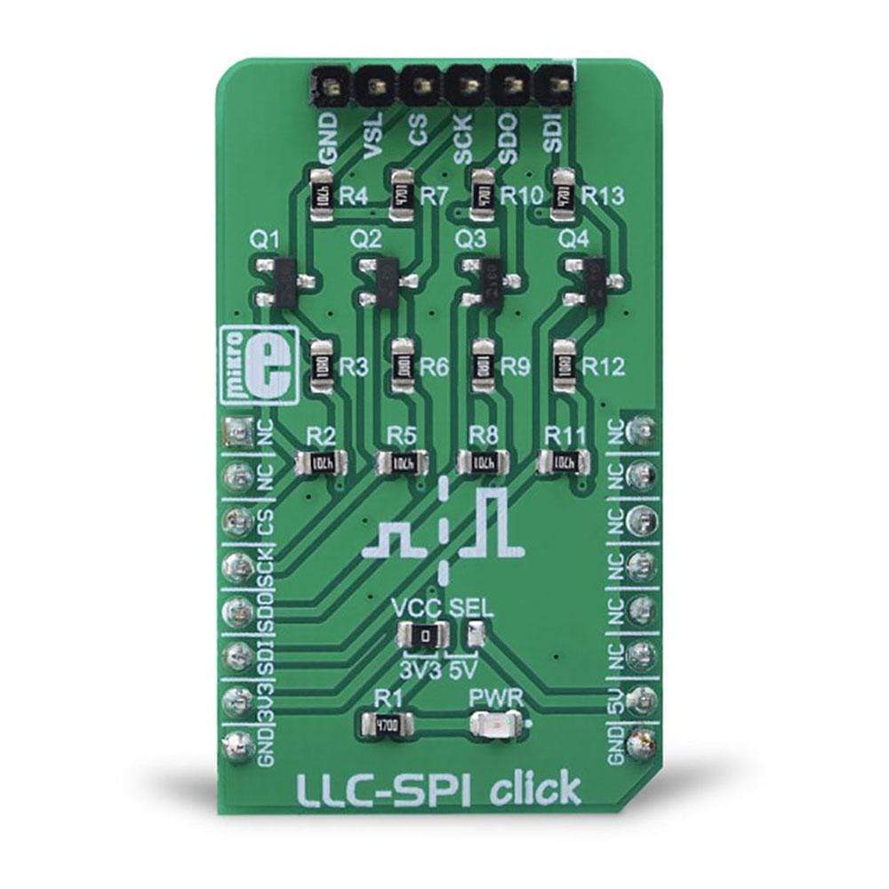
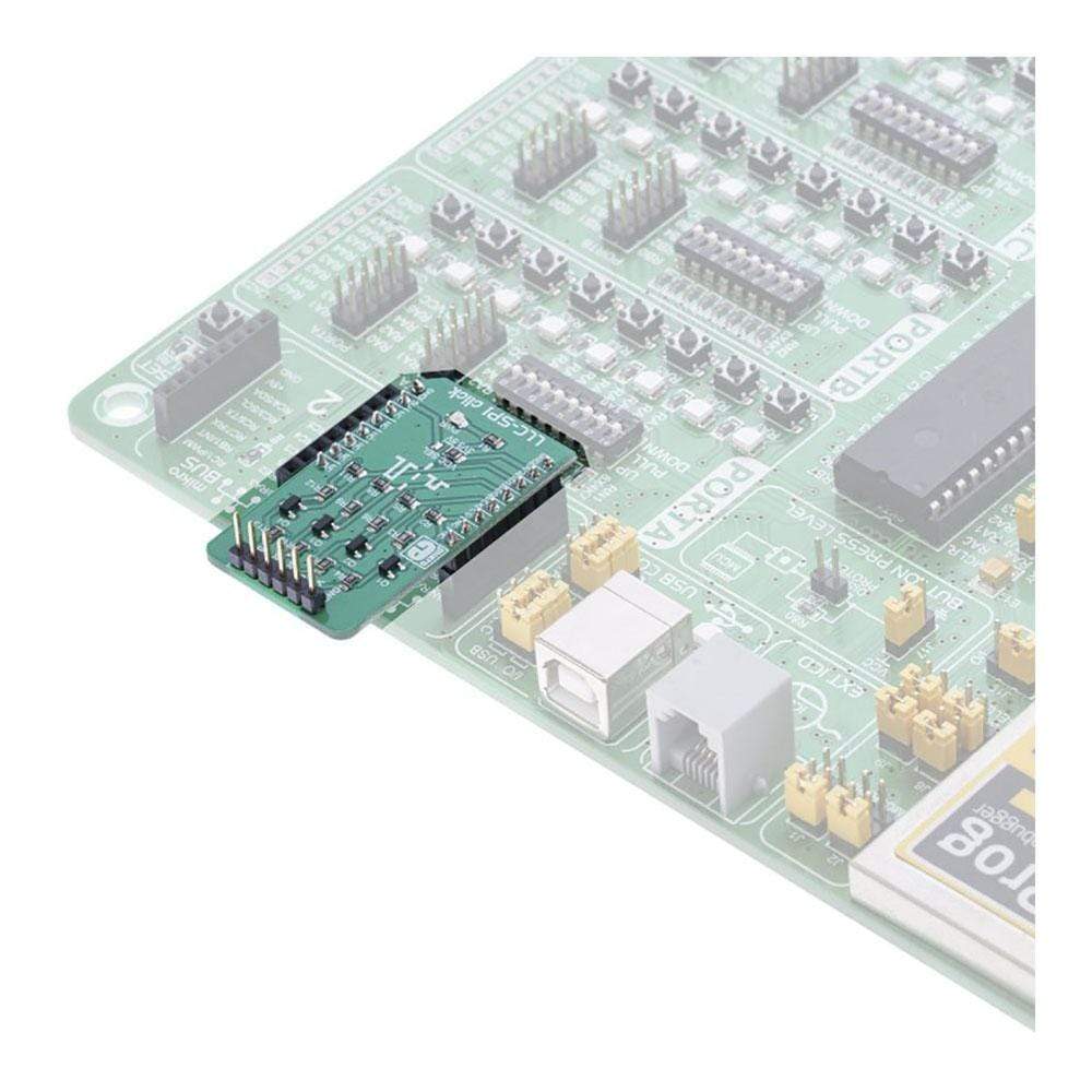
The LLC SPI Click Board™ is a very useful Click Board™ that can be utilized as the level converter for logic signals. The topology of this logic level conversion (LLC) circuit is perfectly suited for SPI communication between devices with unmatched voltages of their logic signals. Although there are some specialised integrated circuits on the market, sometimes it is more convenient to have a simple solution made of just a few passive elements and four MOSFETs.
Downloads
Le LLC SPI Click Board™ est un Click Board™ très utile qui peut être utilisé comme convertisseur de niveau pour les signaux logiques. La topologie de ce circuit de conversion de niveau logique (LLC) est parfaitement adaptée à la communication SPI entre des appareils dont les tensions de leurs signaux logiques sont inégalées. Bien qu'il existe des circuits intégrés spécialisés sur le marché, il est parfois plus pratique d'avoir une solution simple composée de quelques éléments passifs et de quatre MOSFET.
| General Information | |
|---|---|
Part Number (SKU) |
MIKROE-3298
|
Manufacturer |
|
| Physical and Mechanical | |
Weight |
0.019 kg
|
| Other | |
EAN |
8606018714131
|
Frequently Asked Questions
Have a Question?
Be the first to ask a question about this.