


Mikroelektronika d.o.o.
Tableau à clic RN4678
Tableau à clic RN4678
SKU: MIKROE-2545
Impossible de charger la disponibilité du service de retrait

Overview
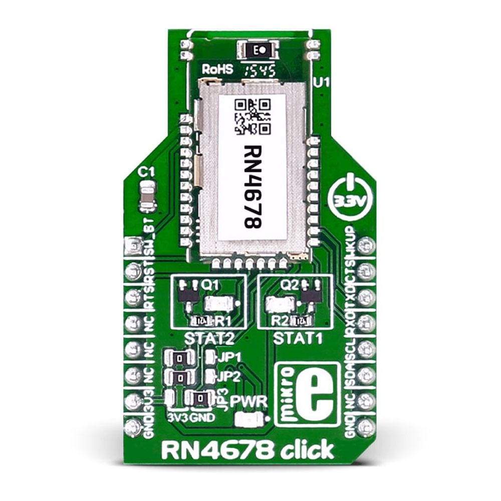
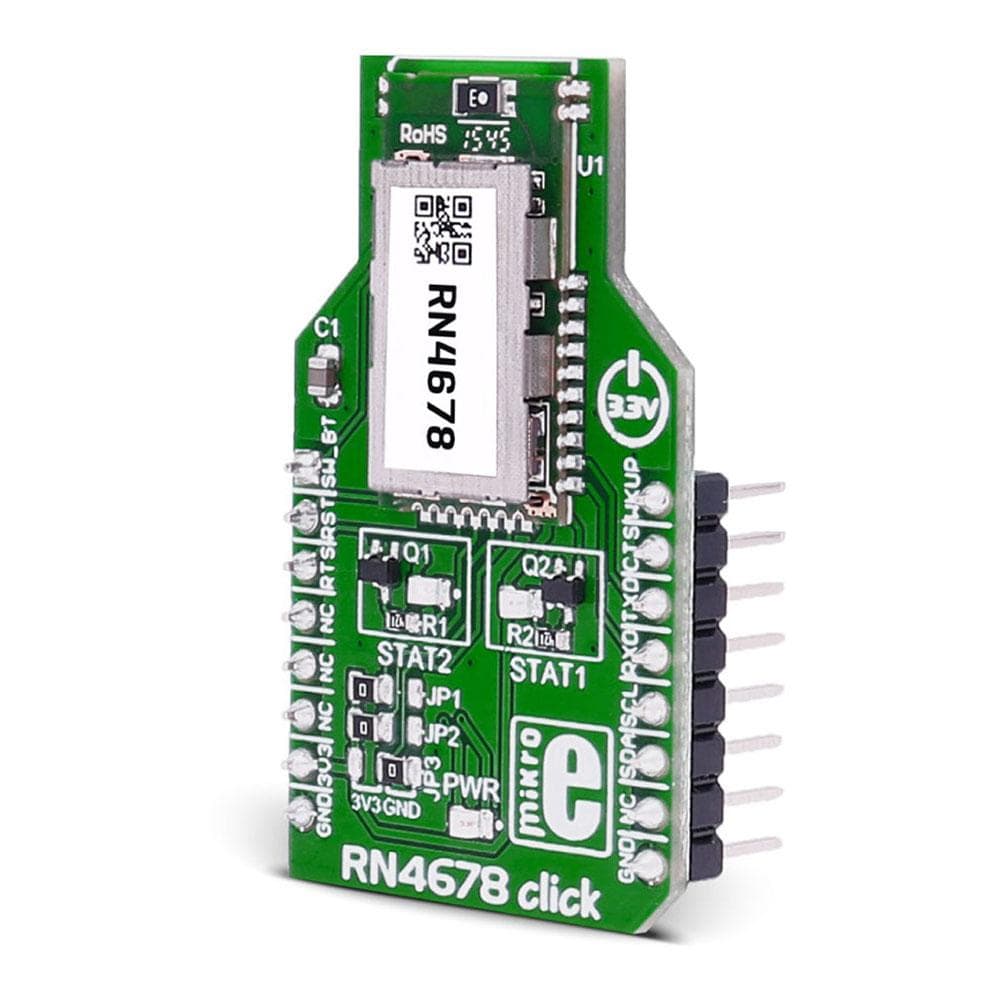
The RN4678 Click Board™ is based on Microchip's RN4678 Bluetooth® 4.2 dual mode module.
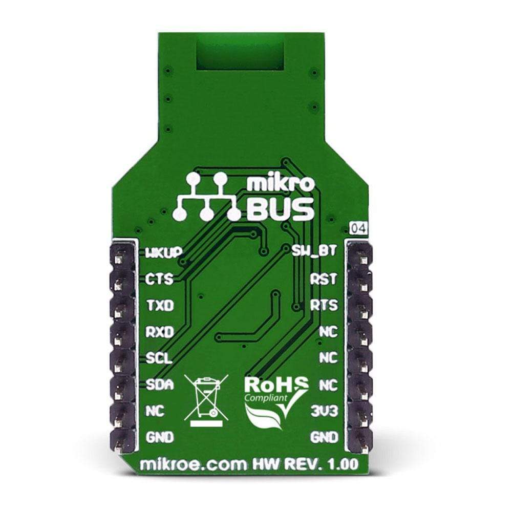
The RN4678 Click Board™ is designed to run on a 3.3V power supply. It communicates with the target microcontroller over I2C and UART interface, with additional functionality provided by the following pins on the mikroBUS™ line: AN, RST, CS, PWM, INT.
Downloads
Le RN4678 Click Board™ est basé sur le module double mode Bluetooth® 4.2 RN4678 de Microchip .
La carte Click Board™ RN4678 est conçue pour fonctionner sur une alimentation de 3,3 V. Elle communique avec le microcontrôleur cible via l'interface I2C et UART, avec des fonctionnalités supplémentaires fournies par les broches suivantes sur la ligne mikroBUS™ : AN, RST, CS, PWM, INT.
| General Information | |
|---|---|
Part Number (SKU) |
MIKROE-2545
|
Manufacturer |
|
| Physical and Mechanical | |
Weight |
0.019 kg
|
| Other | |
EAN |
8606018710423
|
Frequently Asked Questions
Have a Question?
Be the first to ask a question about this.