


Tag-Connect, LLC
Tag Connect TC-LATTICE-10 Adapter
Tag Connect TC-LATTICE-10 Adapter
SKU: TC-LATTICE-10
Couldn't load pickup availability
Key Features
Overview
Downloads
Why Engineers Choose The Tag Connect TC-LATTICE-10 Adapter
Eliminates PCB Connector Costs
Prevents Low-Power Target Issues
Enables Production Programming
Overview
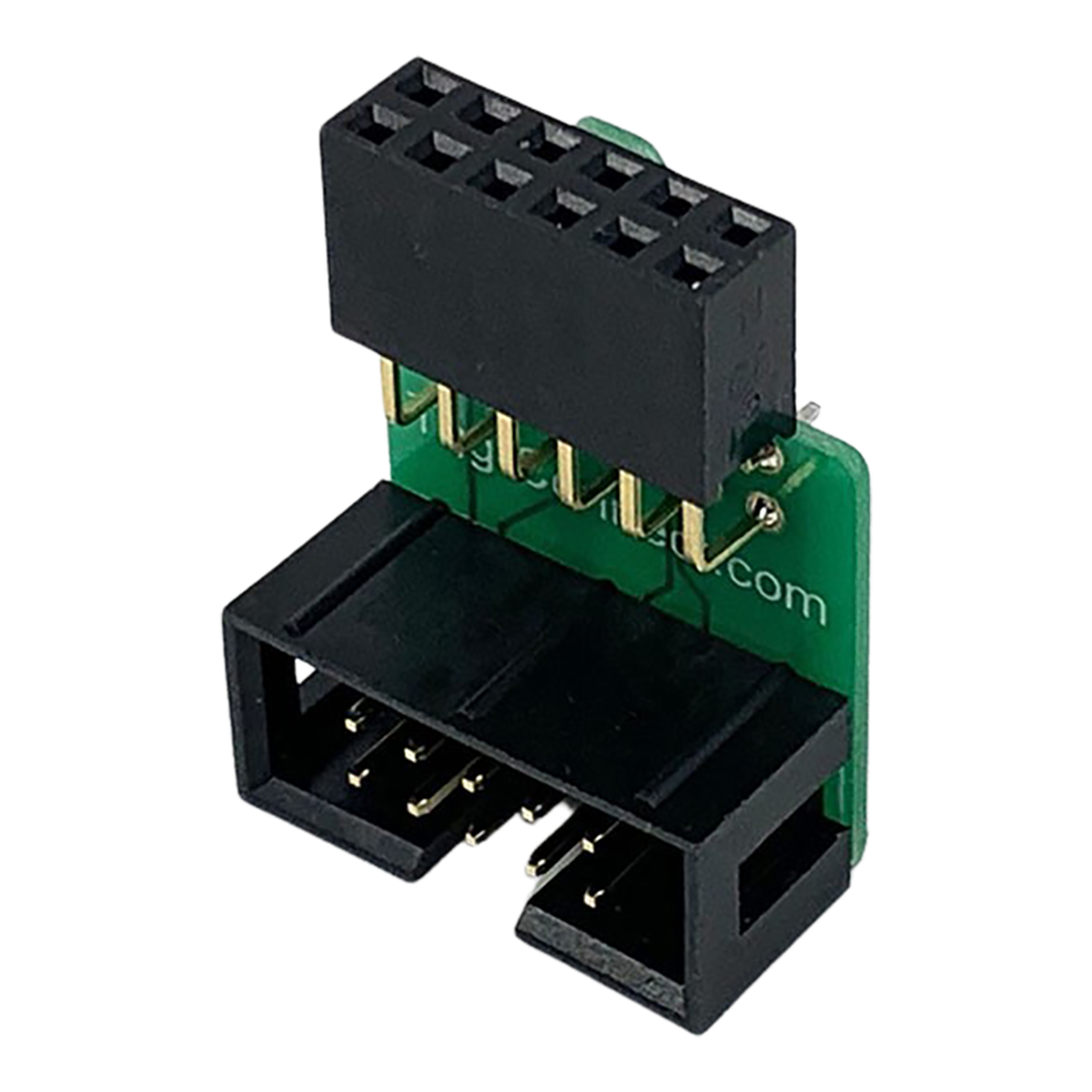
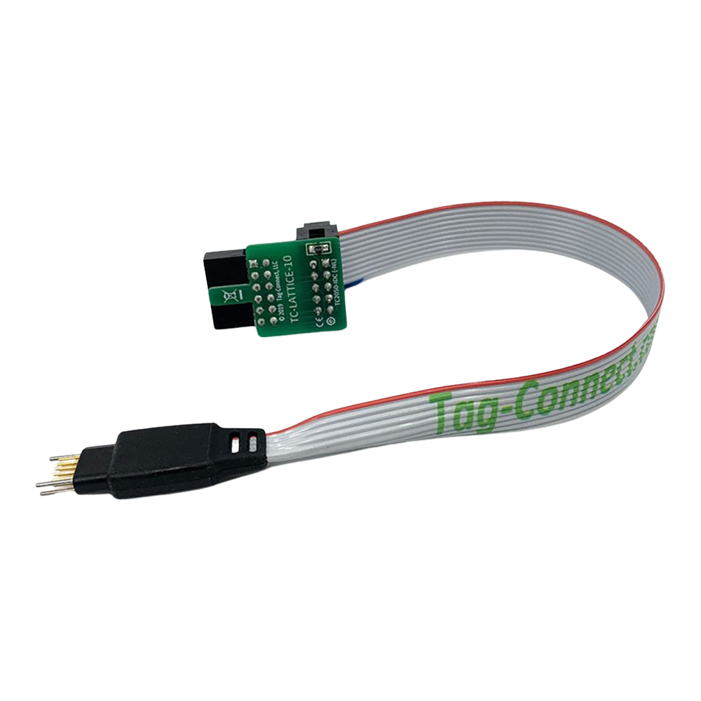
The TC-LATTICE-10 Adapter serves as a crucial interface component enabling engineers to leverage Tag-Connect's space-saving programming solutions with Lattice Semiconductor's HW-USBN-2B programming cable. This adapter eliminates the need for physical programming connectors on target PCBs whilst maintaining full compatibility with Lattice Diamond Programmer and ispVM System software.
Technical Specifications
| Parameter | Specification |
|---|---|
| Input Connector | 12-pin (2×6) 0.1″ female header |
| Output Connector | 10-pin (2×5) 0.1″ male box header |
| Built-in Resistor | 500Ω between VCC and GND |
| Operating Voltage | 1.2V to 3.3V (via HW-USBN-2B) |
| Compatible Cables | TC2050-IDC, TC2050-IDC-NL |
| PCB Dimensions | 25mm × 15mm × 8mm (approx) |
Wiring Quick-Start
Connect the adapter between your HW-USBN-2B programmer and TC2050-IDC cable using the following pin mapping:
| TC2050 Pin | Signal | Description |
|---|---|---|
| 1 | VCC* | Programming voltage supply |
| 2 | TMS | Test Mode Select |
| 3 | GND* | Ground reference |
| 4 | TCK/SCLK | Test Clock/Serial Clock |
| 5 | 5V OUT | 5V output for specific applications |
| 6 | TDO/SO | Test Data Output/Serial Output |
| 7 | DONE | Configuration complete indicator |
| 8 | TDI/SI | Test Data Input/Serial Input |
| 9 | TRST | Test Reset (optional) |
| 10 | ispEN/PROG/SN | Programming enable/Slave select |
*500Ω resistor fitted between VCC and GND on adapter PCB
Installation Procedure
- Ensure your target PCB includes the standard TC2050 footprint with proper pad sizes and locating holes
- Connect the TC-LATTICE-10 adapter to your HW-USBN-2B programmer's 12-pin output connector
- Attach your TC2050-IDC or TC2050-IDC-NL cable to the adapter's 10-pin output
- Position the Tag-Connect cable on your target board's TC2050 footprint
- Launch Lattice Diamond Programmer and detect your target device
Low-Power Target Considerations
Important: The built-in 500Ω resistor addresses a known issue where the HW-USBN-2B can unexpectedly raise VCC on low-power target designs, potentially causing programming failures or device damage.
Without this resistor, low-power targets may experience:
- Unexpected voltage rises during programming
- Programming verification failures
- Inconsistent device behaviour post-programming
Compatible Target Footprint
Your target PCB must include the TC2050 footprint consisting of:
- Ten 0.5mm diameter copper pads arranged in 2×5 configuration
- Two 0.99mm diameter locating holes for mechanical alignment
- Total footprint area of approximately 0.03 square inches
- Minimum copper thickness of 35μm (1oz)
Programming Software Configuration
The adapter requires no special software configuration. Use Lattice Diamond Programmer with standard settings:
1. Select your target device family 2. Choose appropriate programming file (.jed, .bit, .hex) 3. Set operation mode (JTAG/SPI as required) 4. Configure programming options (erase, program, verify) 5. Execute programming sequenceFor command-line programming, use standard ispVM System commands with your regular device configuration files.
Production Programming Integration
The TC-LATTICE-10 adapter enables efficient production programming through:
- Automated test equipment (ATE) compatibility
- Spring-loaded programming fixtures
- High-speed programming cycles (<10 seconds typical)
- Reliable connection repeatability (>100,000 cycles)
Pro Tip: For production environments, consider TC2050-CLIP retention accessories to maintain hands-free programming connections during extended debug sessions.
Troubleshooting Common Issues
| Issue | Probable Cause | Solution |
|---|---|---|
| Device not detected | Poor footprint connection | Verify TC2050 pad cleanliness and cable seating |
| Programming verification fails | Signal integrity issues | Check target board power supply stability |
| Inconsistent programming | Mechanical connection | Ensure proper cable pressure and alignment |
| Software connection errors | Driver issues | Reinstall Lattice programming software and drivers |
| General Information | |
|---|---|
Part Number (SKU) |
TC-LATTICE-10
|
Manufacturer |
|
| Physical and Mechanical | |
Weight |
0.1 kg
|
| Other | |
EAN |
5055383665105
|
Frequently Asked Questions
Have a Question?
Be the first to ask a question about this.