

Overview
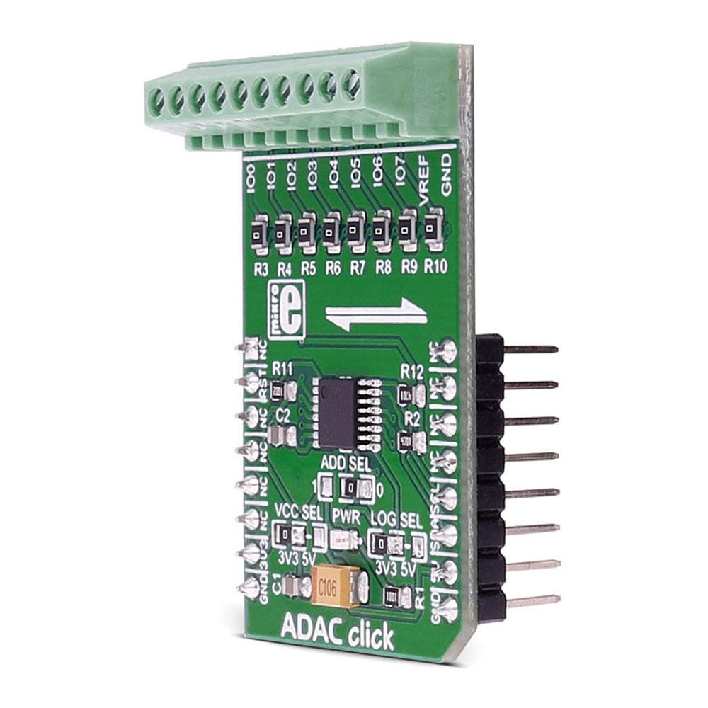
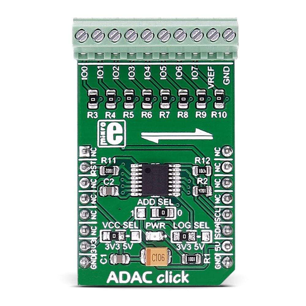
The ADAC Click Board™ is an 8-channel 12-bit ADC, DAC and GPIO. ADAC Click Board™ communicates with the target microcontroller over the I2C interface, with additional functionality provided by the RST pin on the MikroBUS line.
The ADAC Click Board™ is designed to run on either a 3.3V or 5V power supply.
Downloads
The ADAC Click Board™ is an 8-channel 12-bit ADC, DAC and GPIO. It carries the AD5593R configurable ADC/DAC, from Analog Devices. The click is designed to run on either 3.3V or 5V power supply. The ADAC Click Board™ communicates with the target microcontroller over I2C interface, with additional functionality provided by the RST pin on the mikroBUS™ line.
How Does The ADAC Click Board™ Work?
Every channel can be set individually as ADC, DAC, or GPIO. The 12-bit conversion values are readable through I2C.
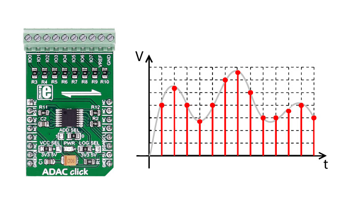
For resetting the IC, use the Reset pin (RST).
AD5593R IC FEATURES
The AD5593R has eight input/output (I/O) pins, which can be independently configured as digital-to-analog converter (DAC) outputs, analog-to-digital converter (ADC) inputs, digital outputs, or digital inputs. When an I/O pin is configured as an analog output, it is driven by a 12-bit DAC. The output range of the DAC is 0 V to VREF or 0 V to 2×V REF.
When an I/O pin is configured as an analog input, it is connected to a 12-bit ADC via an analog multiplexer. The input range of the ADC is 0 V to VREF or 0 V to 2 × VREF. The I/O pins can also be configured to be general-purpose, digital input or output (GPIO) pins.
SPECIFICATIONS
| Type | ADC-DAC |
| Applications | control and monitoring, measurement, etc. |
| On-board modules | AD5593R 8-Channel, 12-Bit, Configurable ADC/DAC |
| Key Features | 8 12-bit DAC channels, 8 12-bit ADC channels |
| Interface | GPIO,I2C |
| Compatibility | mikroBUS |
| Click board size | M (42.9 x 25.4 mm) |
| Input Voltage | 3.3V or 5V |
KEY FEATURES
- AD5593R configurable ADC/DAC
- 8 12-bit DAC channels
- 8 12-bit ADC channels
- 8 general-purpose I/O pins
- I2C interface
- 3.3V or 5V power supply
PINOUT DIAGRAM
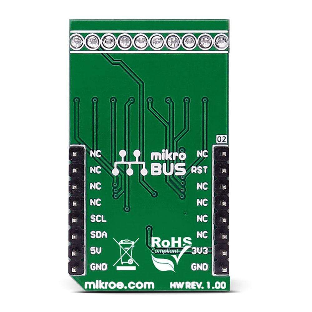
This table shows how the pinout on the ADAC Click Board™ corresponds to the pinout on the mikroBUS™ socket (the latter shown in the two middle columns).
| Notes | Pin |  |
Pin | Notes | |||
|---|---|---|---|---|---|---|---|
| NC | 1 | AN | PWM | 16 | NC | ||
| Active low IC reset | RST | 2 | RST | INT | 15 | NC | |
| NC | 3 | CS | TX | 14 | NC | ||
| NC | 4 | SCK | RX | 13 | NC | ||
| NC | 5 | MISO | SCL | 12 | SCL | I2C serial clock | |
| NC | 6 | MOSI | SDA | 11 | SDA | I2C serial data | |
| Power supply | +3.3V | 7 | 3.3V | 5V | 10 | +5V | Power supply |
| Ground | GND | 8 | GND | GND | 9 | GND | Ground |
ADDITIONAL PINS
| Name | I/O | Description |
|---|---|---|
| IO0 | Multipurpouse IO pin(ADC,DAC,GPIO)channel0 | |
| IO1 | Multipurpouse IO pin(ADC,DAC,GPIO)channel1 | |
| IO2 | Multipurpouse IO pin(ADC,DAC,GPIO)channel2 | |
| IO3 | Multipurpouse IO pin(ADC,DAC,GPIO)channel3 | |
| IO4 | Multipurpouse IO pin(ADC,DAC,GPIO)channel4 | |
| IO5 | Multipurpouse IO pin(ADC,DAC,GPIO)channel5 | |
| IO6 | Multipurpouse IO pin(ADC,DAC,GPIO)channel6 | |
| IO7 | Multipurpouse IO pin(ADC,DAC,GPIO)channel7 | |
| VREF | OPTIONAL | Used as input for connecting external VREF or output 2.5V from internal |
| GND | OPTIONAL | Used for external connection to GND if VREF input is used |
JUMPERS AND SETTINGS
| Designator | Name | Default Position | Default Option | Description |
|---|---|---|---|---|
| ADD SEL | Address bit | 0 | 3V3 | I2C slave address selection, set LSB of slave address 0010001x left pos, 0010000x right pos, (x=R/W) |
| VCC SEL | Power supply | 3V3 | Supply Voltage Selection 3V3/5V, left position 3v3, right position 5v | |
| LOG SEL | Interface power supply | 3V3 | Logic Level Voltage Selection 3V3/5V, left position 3v3, right position 5v |
| General Information | |
|---|---|
Part Number (SKU) |
MIKROE-2690
|
Manufacturer |
|
| Physical and Mechanical | |
Weight |
0.03 kg
|
| Other | |
Country of Origin |
|
HS Code Customs Tariff code
|
|
EAN |
8606018710874
|
Warranty |
|
Frequently Asked Questions
Have a Question?
Be the first to ask a question about this.

