

Mikroelektronika d.o.o.
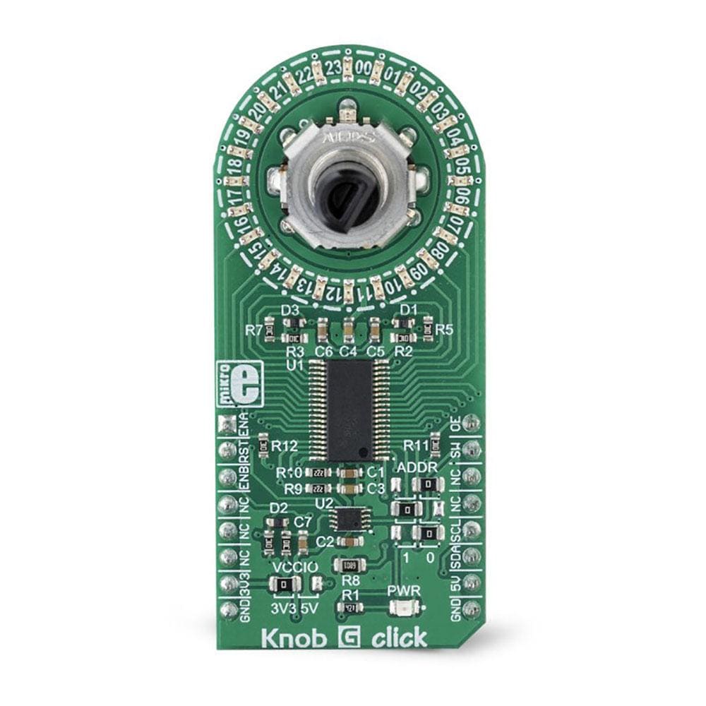
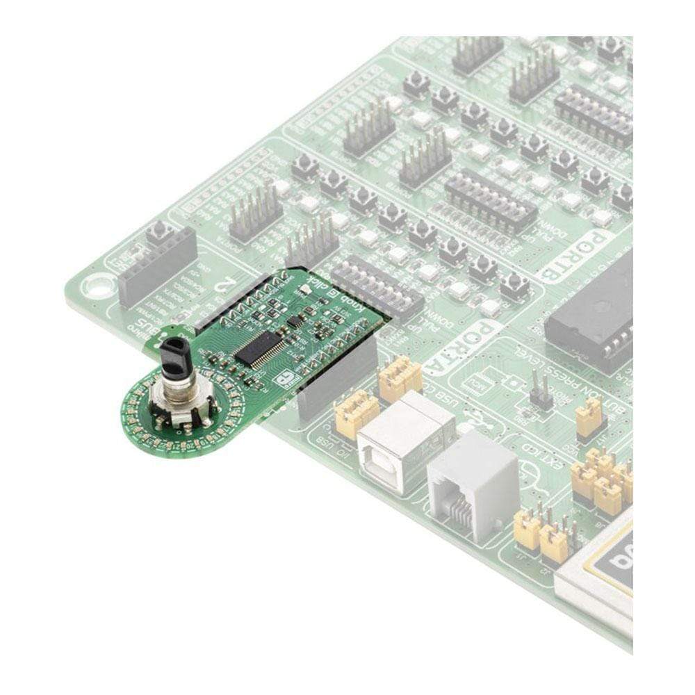
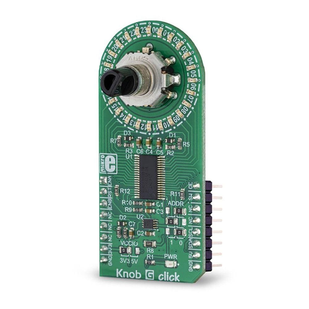
Knob G Click Board™
Knob G Click Board™
SKU: MIKROE-3299
Couldn't load pickup availability


Overview
The Knob G Click Board™ features a combination of high-quality quadrature rotary encoder, and a LED ring composed of 24 individual green LEDs. Outputs of the rotary encoder are processed by a debouncing circuitry, which ensures reliable switching action, making the encoder directly usable in interrupt service routines (ISR) without the need for a bulky debouncing code. The 24-segment LED ring is driven by an advanced and flexible LED driver IC, which can dim each LED individually, allowing various lighting effects to be programmed. The LED ring is independent of the encoder, and it can be used as a very flexible position or value indicator.
Downloads
Featuring highly advanced LED driver IC which offers an unparalleled flexibility, 24 individual LEDs which form a ring around the encoder, a high-quality rotary encoder with push-button by ALPS, and the debouncing circuitry based on a triple Schmitt trigger IC, the Knob G Click Board™ is an ideal solution for building various HMI applications where precise input is required. Also, it can be used to add various interesting visual effects to any application.
How Does The Knob G Click Board™ Work?
The Knob G Click Board™ consists of two distinctive sections: the first section is the rotary quadrature encoder with its outputs routed to the GPIO pins of the mikroBUS. The encoder is debounced by a dedicated circuitry composed of passive elements and a triple inverting Schmitt trigger IC. The second section is the LED driver IC, with accompanying LEDs positioned in a form of a ring around the encoder, making them perfectly suited for encoder position indicators.
The Knob G Click Board™ uses the EC12D, a 15-pulse incremental rotary encoder with a push-button, from ALPS. This encoder has very good mechanical specifications: debouncing time for its internal switches goes down to 2ms, and it can withstand a huge number of switching cycles, up to 30,000. The supporting debouncing circuitry allows contacts to fully settle before the output is triggered.
When encoder contacts are closed, the capacitor will start to discharge through the resistor, via the contacts, and to the GND. The Schmitt trigger connected to the capacitor will output a LOW logic level when its low voltage threshold level is reached; and vice versa - when encoder contacts are open, the capacitor will start to charge through the resistor, and the Schmitt trigger will output a HIGH logic level, when its high voltage threshold level is reached. This allows reading the states of two encoder contacts and one push-button contact directly from the code, with no bulky software debouncing applied. This makes Knob G click usable directly within the the interrupt-on-change ISR, allowing an absolute accuracy and no skipped pulses (which might occur when a regular software polling technique is used). Output pins of the encoder contacts are labelled as ENA and ENB for the quadrature encoder contacts, and SW for the push-button contact. These pins are routed to the AN, CS, and INT pin of the Mirko BUS, respectively.
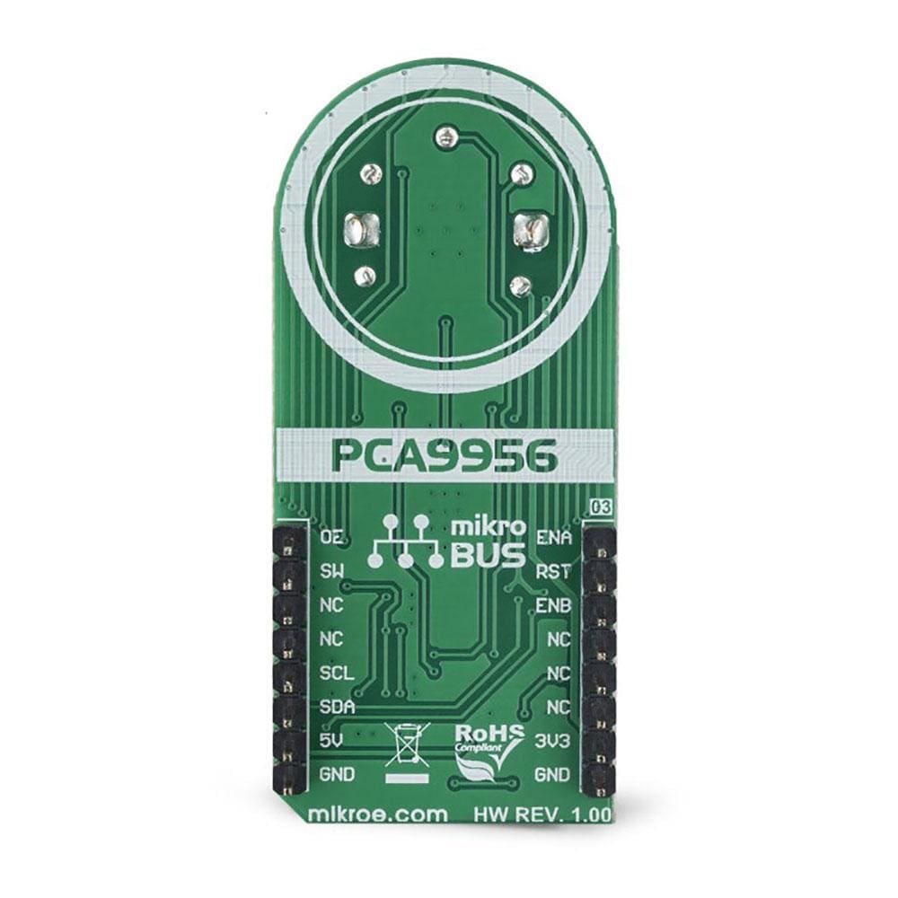
The LED ring is composed of 24 individual green LEDs which are driven by the PCA9956B, an 8-bit, 24-channel, constant current LED driver, from NXP. This driver IC has many LED driving features, including constant current sinking capability, which greatly simplifies the design: maximum current through LEDs is determined by a single resistor. The PCA9956B has registers for controlling each channel individually, along with a single register which controls all channels at once. It supports PWM-mode dimming, as well as the current-mode dimming (by scaling down the maximum LED current). The PCA9956B can use a lower frequency signal from a secondary integrated PWM oscillator to modulate the PWM dimming signal. While the PWM frequency of the driver is fixed at 31.25kHz reducing the visible LED flickering completely, the modulating low-frequency signal can range from 0 to 122Hz, allowing interesting blinking effects to be produced without using the computing power of the microcontroller (MCU). The driver produces smooth dimming of LEDs, since the resolution of the PWM duty cycle is 8 bits. More details and features can be found found in the PCA9956B datasheet, in the download section, below.
The OE pin of the PCA9956B is routed to the PWM pin of the mikroBUS. When a LOW logic level is applied to the OE pin, LED outputs will be enabled. This pin is pulled to a HIGH logic level by a resistor. The OE pin can also be driven by an external PWM signal, offering an alternative way of dimming all LEDs at once.
LED driver IC can be reset by pulling the RST pin to a LOW logic level. This pin is pulled to a HIGH level by the resistor. The reset pulse can be very short (2.5 µs) but the device will not be ready for another 1.5 ms after the pulse. Besides the hardware reset, the PCA9956B also supports a software reset, which is required if the device is going to be operated in the fast I2C mode (including clock speed above 100kHz). The datasheet of the PCA9956B offers a detailed explanation on performing the software reset and using the fast I2C mode (FM+)
The PCA9956B IC uses the 3.3V rail of the mikroBUS as the LED power supply, so there is no significant voltage drop causing thermal dissipation. However, turning all LEDs ON at once with the maximum current set in the current registers, might cause the Knob G click to dissipate some heat. This is expected, as the thermal dissipation of each channel is adding up to the sum dissipation of the entire IC. The PCA9956B IC features thermal shutdown protection, along with the set of error reporting features. The PCA9956B can report both open-circuit event and short-circuit event for each LED. These errors will be written in the ERR registers, one for each LED channel. The datasheet explains how to interpret the values of these registers.
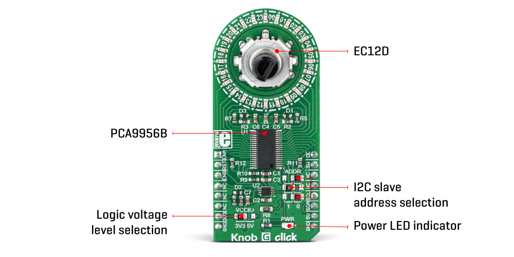
Slave I2C address of the PCA9956B device can be selected by using three SMD jumpers, grouped under the ADDR label. The PCA9956B allows its slave I2C address to be selected from a wide range of 125 different values. Each of the address pins (A0 to A3) can be left floating, pulled up, pulled down and shorted to VCC or GND. However, some I2C addresses are reserved, so they should be used with care. The datasheet of the PCA9956B offers tables with resistor values for each state of the address pins and reserved I2C addresses. Knob G click uses three 0 Ω SMD jumpers to set the states of these address pins.
The logic voltage level can be selected by the SMD jumper, labelled as VCCIO. This jumper determines levels for the logic signals from Schmitt triggers, as well as for the I2C interface of the Knob G Click Board™ . This allows it to be interfaced with a wide range of different MCUs, both compatible with 3.3V and 5V logic voltage levels.
SPECIFICATIONS
| Type | Rotary encoder |
| Applications | The Knob G Click Board™ is an ideal solution for building various HMI applications, where a precise input is required. Also, it can also be used to add various interesting visual effects to any application. |
| On-board modules | PCA9956B, an 8-bit, 24-channel, constant current LED driver, from NXP; 74HC3G14DC, a triple inverting Schmitt trigger IC, from Nexperia |
| Key Features | A reliable symmetrical debouncing circuit, a very flexible and powerful PWM LED driver which features several different dimming options, constant current through LEDs can be selected by a single resistor, smooth dimming in 256 steps for each LED channel, 24-segment LED ring that can be used for the visual feedback, etc. |
| Interface | GPIO,I2C |
| Compatibility | mikroBUS |
| Click board size | L (57.15 x 25.4 mm) |
| Input Voltage | 3.3V or 5V |
PINOUT DIAGRAM
This table shows how the pinout on the Knob G Click corresponds to the pinout on the mikroBUS™ socket (the latter shown in the two middle columns).
| Notes | Pin | Pin | Notes | ||||
|---|---|---|---|---|---|---|---|
| Encoder OUT A | ENA | 1 | AN | PWM | 16 | OE | Control PWM Signal |
| PCA9956B Reset | RST | 2 | RST | INT | 15 | SW | Encoder Button OUT |
| Encoder OUT B | ENB | 3 | CS | RX | 14 | NC | |
| NC | 4 | SCK | TX | 13 | NC | ||
| NC | 5 | MISO | SCL | 12 | SCL | I2C Clock | |
| NC | 6 | MOSI | SDA | 11 | SDA | I2C Data | |
| Power supply | 3V3 | 7 | 3.3V | 5V | 10 | 5V | Power supply |
| Ground | GND | 8 | GND | GND | 9 | GND | Ground |
ONBOARD SETTINGS AND INDICATORS
| Label | Name | Default | Description |
|---|---|---|---|
| PWR | PWR | - | Power LED indicator |
| JP0, JP2 | ADDR | Right | I2C slave address selection: left position GND (0), right position VCC (1) |
| JP1 | ADDR | Left | I2C slave address selection: left position GND (0), right position VCC (1) |
| JP3 | VCCIO | Left | Logic voltage level selection: left position 3.3V, right position 5V |
Note: please consult the datasheet of the PCA9956B if you need to change the default I2C slave address
| General Information | |
|---|---|
Part Number (SKU) |
MIKROE-3299
|
Manufacturer |
|
| Physical and Mechanical | |
Weight |
0.022 kg
|
| Other | |
EAN |
8606018714148
|
Frequently Asked Questions
Have a Question?
Be the first to ask a question about this.