


Mikroelektronika d.o.o.
GainAMP Click Board™
GainAMP Click Board™
SKU: MIKROE-2555
Couldn't load pickup availability
Overview
The GainAMP Click Board™ is based on the LTC6912 dual-channel, low noise, digitally programmable gain amplifier (PGA).
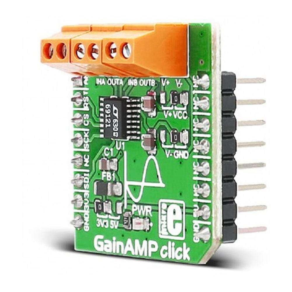
The GainAMP Click Board™ is designed to work on a 3.3V or 5V power supply. It communicates with the target MCU over the SPI interface, with additional functionality provided by the following pins on the mikroBUS line: AN, RST.
Downloads
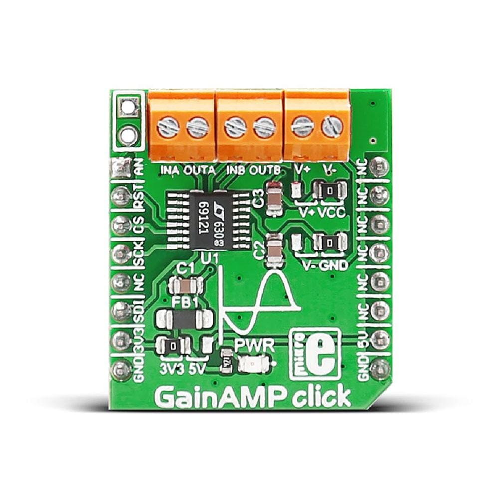
The GainAMP Click Board™ carries the LTC6912 dual-channel, low noise, digitally programmable gain amplifier (PGA), from Analog Devices. The click is designed to work on either a 3.3V or 5V power supply. It communicates with the target MCU over the SPI interface, with additional functionality provided by the following pins on the mikroBUS™ line: AN, RST.
The GainAMP Click Board™ also features three pairs of screw terminals and a power indication LED.
How Does The GainAMP Click Board™ Work?
The gains for both channels are independently programmable, using a 3-wire SPI interface to select voltage gains of 0, 1, 2, 5, 10, 20, 50, and 100V/V (LTC6912-1). All gains are inverting.
The LTC®6912 consists of 2 matched amplifiers with rail-to-rail outputs. When operated with unity gain, they will also process rail-to-rail input signals.
A half-supply reference generated internally at the AGND pin supports single power supply applications. Operating from single or split supplies from 2.7V to 10.5V total.
Programmable Gain Amplifier
A programmable gain amplifier (PGA) is an electronic amplifier whose gain can be controlled externally (by analogue or digital signals).
Specifications
| Type | Amplifier |
| Applications | Data Acquisition Systems, Dynamic Gain Changing, Automatic Ranging Circuits, Automatic Gain Control. |
| On-board modules | LTC®6912 dual-channel gain amplifier |
| Key Features | Rail-to-Rail Output Swing, Rail-to-Rail Input Range, 2 Channels with Independent Gain Control, Three pairs of screw terminals, 3-wire SPI interface |
| Interface | Analog,GPIO,SPI |
| Compatibility | mikroBUS |
| Click board size | S (28.6 x 25.4 mm) |
| Input Voltage | 3.3V or 5V |
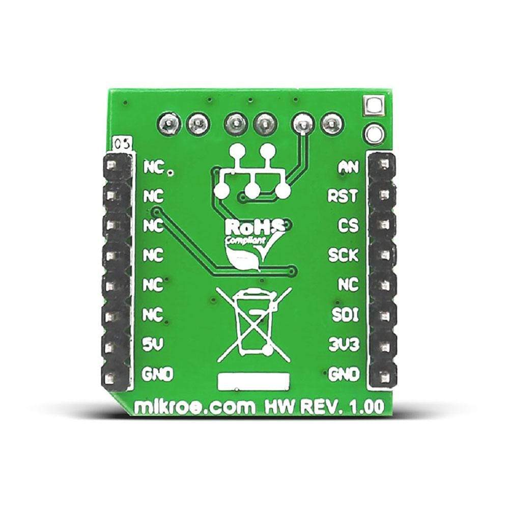
Pinout Diagram
This table shows how the pinout on GainAMP click corresponds to the pinout on the mikroBUS™ socket (the latter shown in the two middle columns).
| Notes | Pin | Pin | Notes | ||||
|---|---|---|---|---|---|---|---|
| Analog input | AN_IN | 1 | AN | PWM | 16 | NC | |
| Shut down | SHDN | 2 | RST | INT | 15 | NC | |
| Chip select | SPI_CS | 3 | CS | TX | 14 | NC | |
| SPI Clock Input | SPI_CLK | 4 | SCK | RX | 13 | NC | |
| NC | 5 | MISO | SCL | 12 | NC | ||
| SPI Master Output Slave Input | SPI_MOSI | 6 | MOSI | SDA | 11 | NC | |
| Power supply | +3.3V | 7 | 3.3V | 5V | 10 | +5V | Power supply |
| Ground | GND | 8 | GND | GND | 9 | GND | Ground |
Maximum Ratings
| Description | Min | Typ | Max | Unit |
|---|---|---|---|---|
| Total Supply Voltage (V+ to V–) | 11V | V | ||
| Input Current | ±10 | mA | ||
| Operating Temperature Range | –40°C | 85°C |
Jumpers and settings
| Designator | Name | Default Position | Default Option | Description |
|---|---|---|---|---|
| JP1 | AN_sel | ON | AN | Analog input jumper. |
| JP2 | V+ | Left | VCC | V+ selection. |
| JP3 | V- | Left | GND | V- selection. |
| General Information | |
|---|---|
Part Number (SKU) |
MIKROE-2555
|
Manufacturer |
|
| Physical and Mechanical | |
Weight |
0.02 kg
|
| Other | |
EAN |
8606018710225
|
Frequently Asked Questions
Have a Question?
Be the first to ask a question about this.