

Mikroelektronika d.o.o.
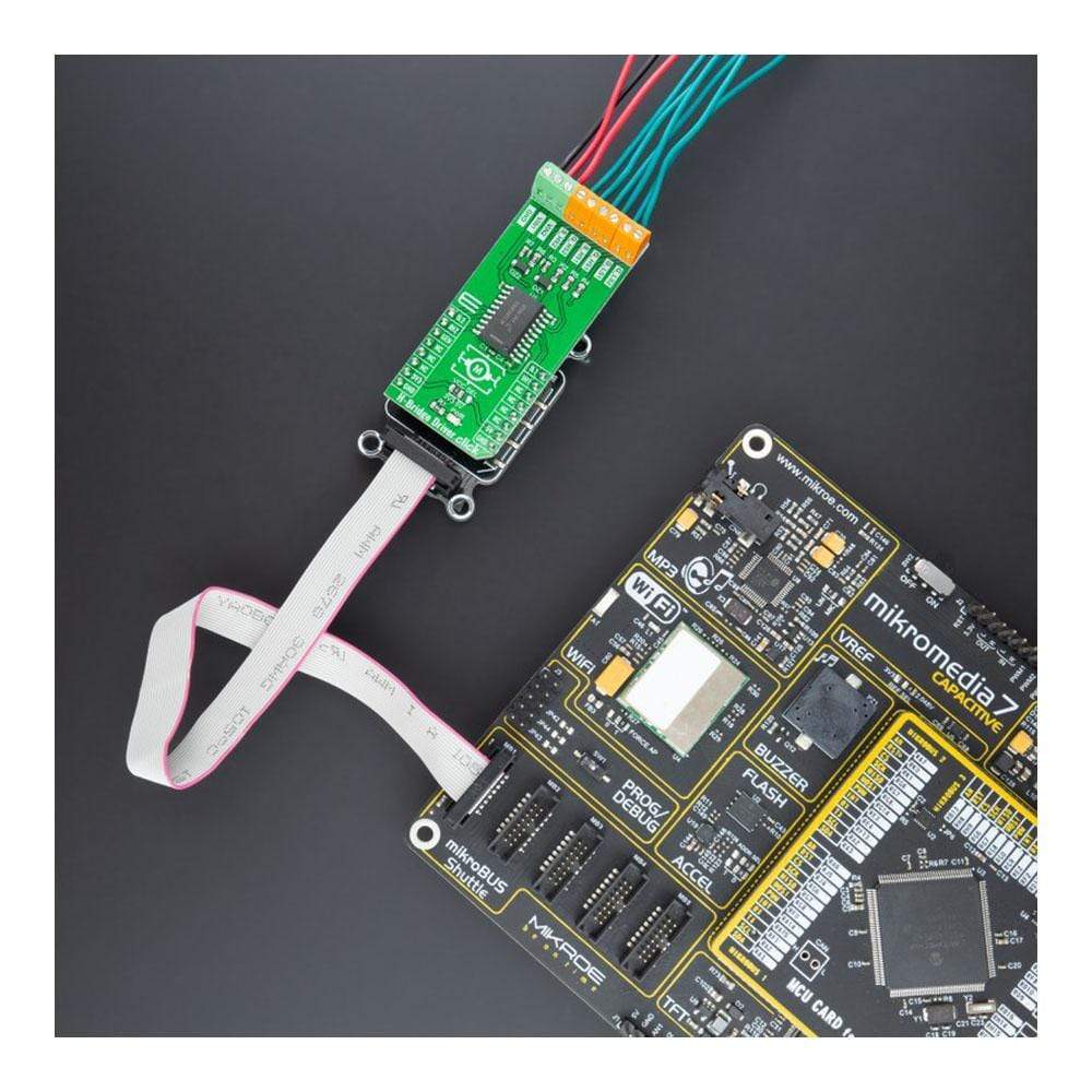
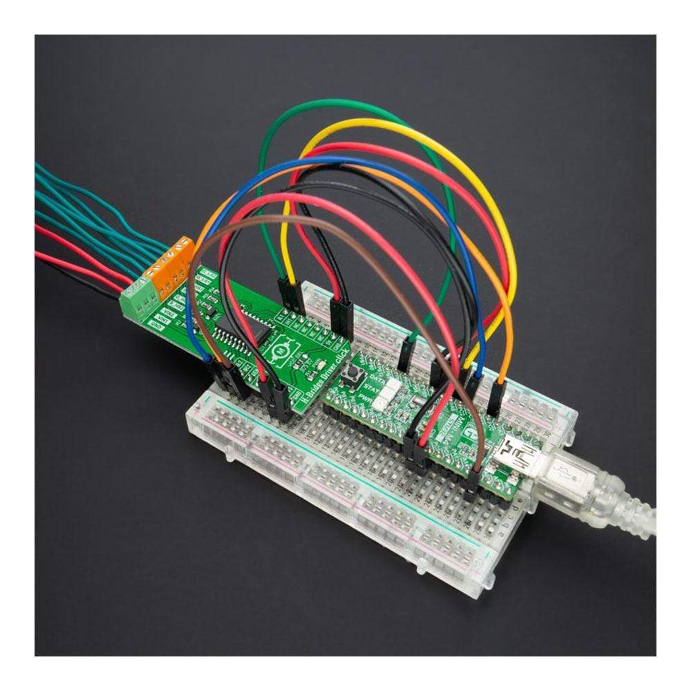
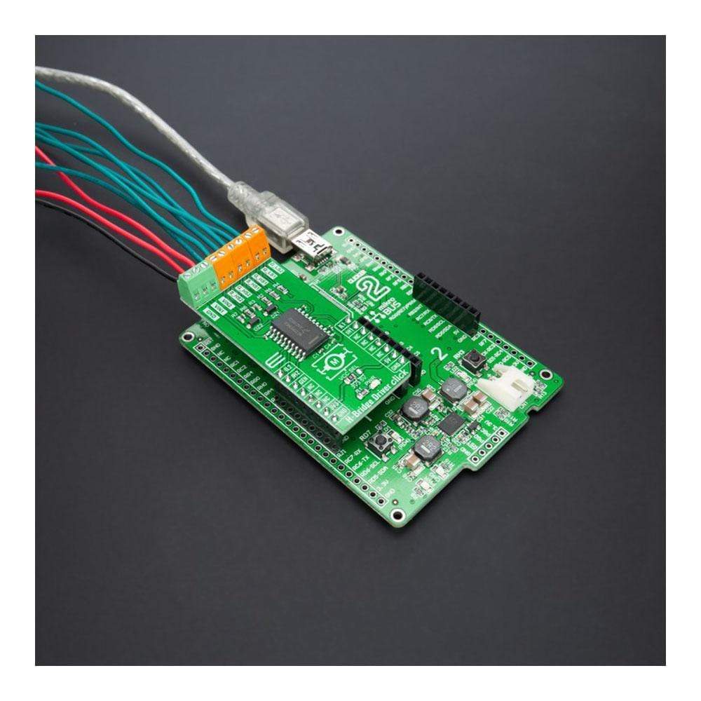
H-Bridge Driver Click Board™
H-Bridge Driver Click Board™
SKU: MIKROE-4696
Couldn't load pickup availability


Overview
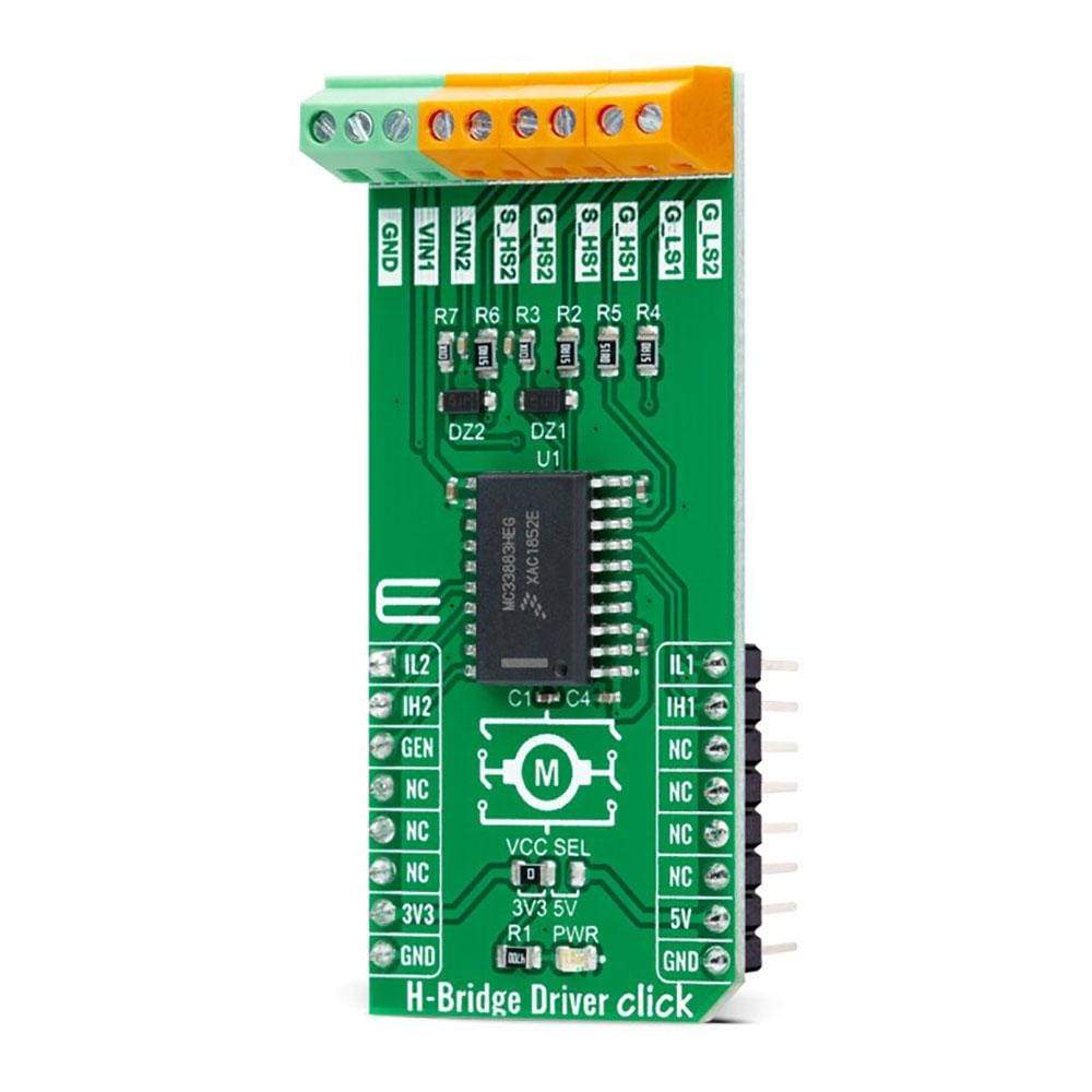
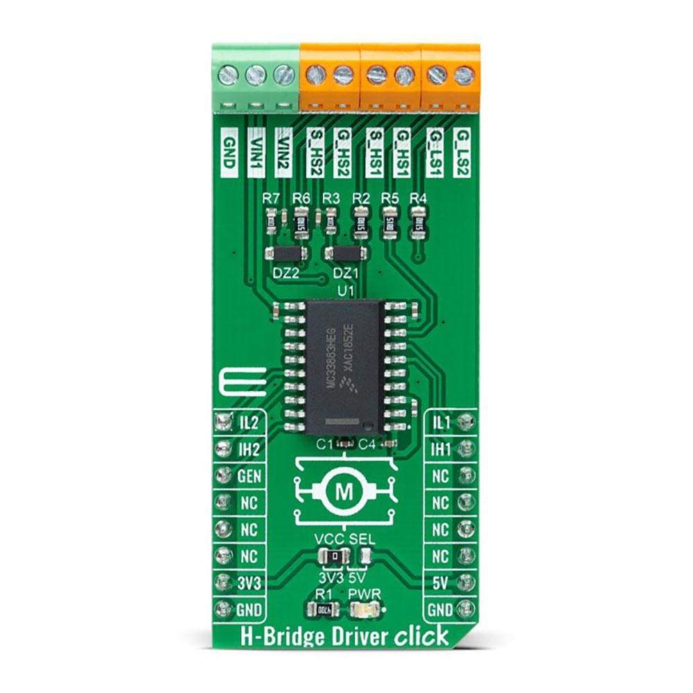
The H-Bridge Driver Click Board™ is a compact add-on board that contains an H-bridge gate driver, also known as a full-bridge pre-driver. This board features the MC33883, an H-Bridge gate driver with an integrated charge pump and independent high and low side gate drive channels from NXP Semiconductors. The gate driver channels are independently controlled by four separate input pins, allowing the device to be optionally configured as two independent high side gate drivers and two independent low side gate drivers. Gate driver outputs can source and sink up to 1.0A peak current pulses, permitting large gate-charge MOSFETs to be driven and/or high pulse-width modulation (PWM) frequencies to be utilized.
The H-Bridge Driver Click Board™ is suitable for automotive engine applications (electric pumps), energy storage systems (ESS), uninterruptible power supply (UPS), and more.
Downloads
How Does The H-Bridge Driver Click Board™ Work?
The H-Bridge Driver Click Board™ as its foundation uses the MC33883, an H-bridge gate driver (or full-bridge pre-driver) with integrated charge pump and independent high and low-side driver channels from NXP Semiconductors. Gate driver outputs can source and sink up to 1.0A peak current pulses, permitting large gate-charge MOSFETs to be driven and/or high pulse-width modulation (PWM) frequencies to be utilized. It also supports a Sleep mode of operation with its low supply current, typical of 10μA.

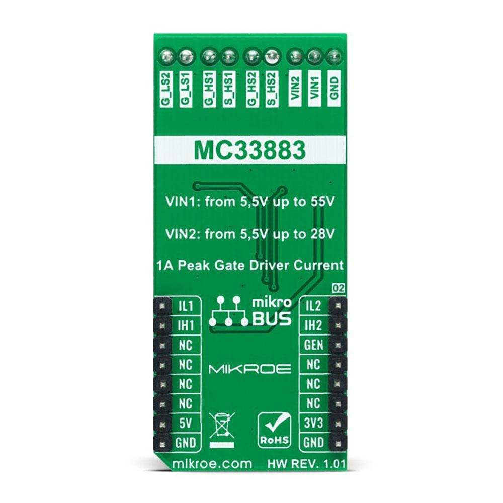
The VIN1 and VIN2 terminals are the power supply inputs to the device. VIN1 is used for the output high-side drivers and the charge pump, while VIN2 is used for the linear regulation. They can be connected together or with different voltage values with VIN1 up to 45V and VIN2 up to 28V. These pins also have under-voltage (UV) and overvoltage (OV) shutdown features. If one of the supply voltage drops below the under-voltage threshold or rises above the overvoltage threshold, the gate outputs are switched low to switch off the external MOSFETs. When the supply returns to a level above the UV threshold or below the OV threshold, the device resumes normal operation according to the established condition of the input pins.
The gate driver channels are independently controlled by four separate pins, routed to the RST, AN, PWM, and INT pins of the mikroBUS™ socket. Those pins allow the device to be optionally configured as two independent high side gate drivers and two independent low side gate drivers. In addition, it also has a pin used to place the device in Sleep mode. When the GEN pin, routed to the CS pin of the mikroBUS™ socket, is in a logic low state, the device is in Sleep mode; otherwise, it is fully operational.
The H-Bridge Driver Click Board™ can operate with both 3.3V and 5V logic voltage levels selected via the VCC SEL jumper. This way, it allows both 3.3V and 5V capable MCUs to use the GPIO communication lines properly. However, the Click board™ comes equipped with a library containing easy-to-use functions and an example code that can be used, as a reference, for further development.
SPECIFICATIONS
| Type | Brushed |
| Applications | The H-Bridge Driver Click Board™ can be used for automotive engine applications (electric pumps), energy storage systems (ESS), uninterruptible power supply (UPS), and more. |
| On-board modules | MC33883 - H-bridge gate driver (or full-bridge pre-driver) with integrated charge pump and independent high and low-side driver channels from NXP Semiconductors |
| Key Features | Full-bridge pre-driver, built-in high side charge pump, UVLO and OVLO features, Sleep mode, PWM up to 100kHz, and more. |
| Interface | GPIO |
| Compatibility | mikroBUS |
| Click board size | L (57.15 x 25.4 mm) |
| Input Voltage | 3.3V or 5V, External |
PINOUT DIAGRAM
This table shows how the pinout on the H-Bridge Driver Click Board™ corresponds to the pinout on the mikroBUS™ socket (the latter shown in the two middle columns).
| Notes | Pin | Pin | Notes | ||||
|---|---|---|---|---|---|---|---|
| Input Low Side 2 | IL2 | 1 | AN | PWM | 16 | IL1 | Input Low Side 1 |
| Input High Side 2 | IH2 | 2 | RST | INT | 15 | IH1 | Input High Side 1 |
| Global Enable | GEN | 3 | CS | RX | 14 | NC | |
| NC | 4 | SCK | TX | 13 | NC | ||
| NC | 5 | MISO | SCL | 12 | NC | ||
| NC | 6 | MOSI | SDA | 11 | NC | ||
| Power Supply | 3.3V | 7 | 3.3V | 5V | 10 | 5V | Power Supply |
| Ground | GND | 8 | GND | GND | 9 | GND | Ground |
ONBOARD SETTINGS AND INDICATORS
| Label | Name | Default | Description |
|---|---|---|---|
| LD1 | PWR | - | Power LED Indicator |
| JP1 | VCC SEL | Left | Logic Level Voltage Selection 3V3/5V: Left position 3V3, Right position 5V |
H-BRIDGE DRIVER CLICK ELECTRICAL SPECIFICATIONS
| Description | Min | Typ | Max | Unit |
|---|---|---|---|---|
| Supply Voltage VCC | 3.3 | - | 5 | V |
| Supply Voltage VIN1 | - | - | 45 | V |
| Supply Voltage VIN2 | - | - | 28 | V |
| Operating Temperature Range | -40 | +25 | +125 | °C |
| General Information | |
|---|---|
Part Number (SKU) |
MIKROE-4696
|
Manufacturer |
|
| Physical and Mechanical | |
Weight |
0.02 kg
|
| Other | |
EAN |
8606027383182
|
Frequently Asked Questions
Have a Question?
Be the first to ask a question about this.