


Mikroelektronika d.o.o.
nvSRAM Click Board™
nvSRAM Click Board™
SKU: MIKROE-4441
Couldn't load pickup availability


Overview
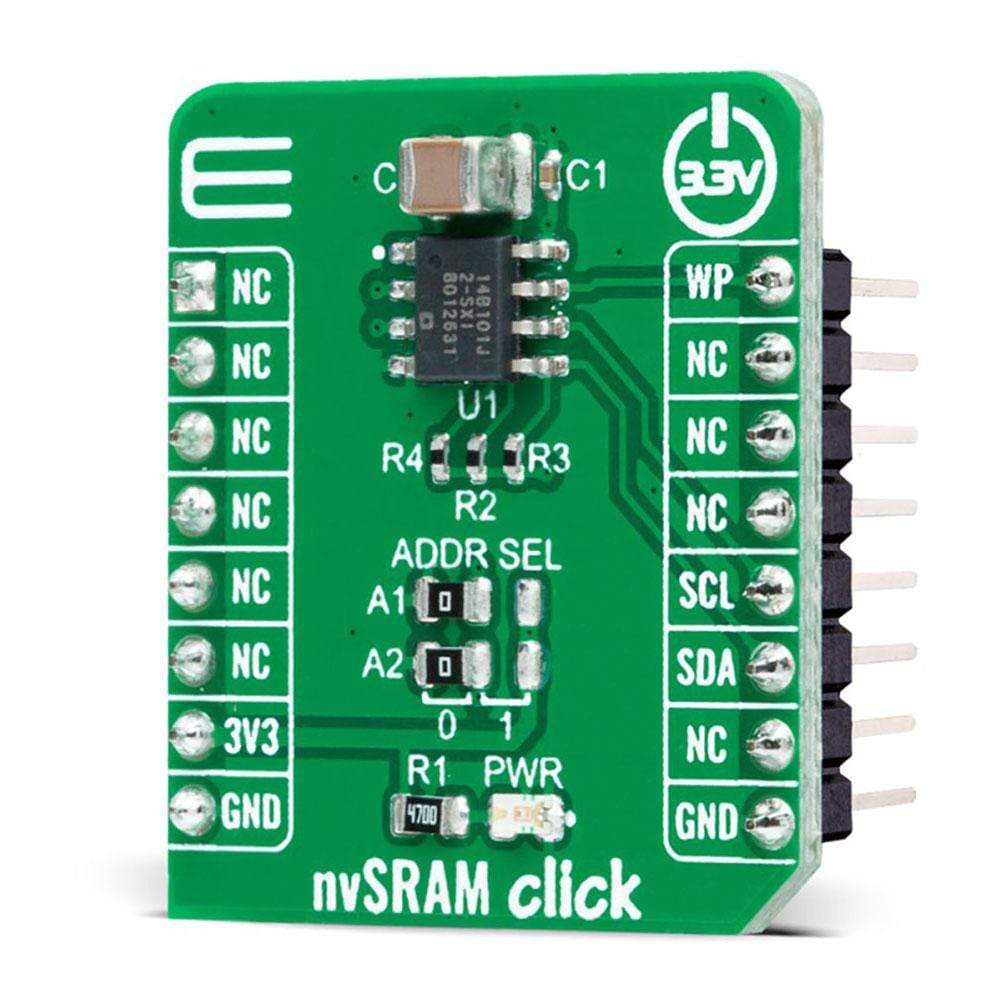
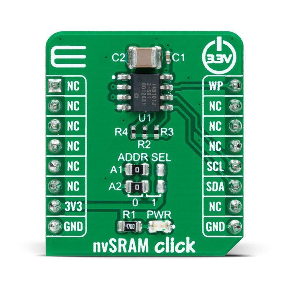
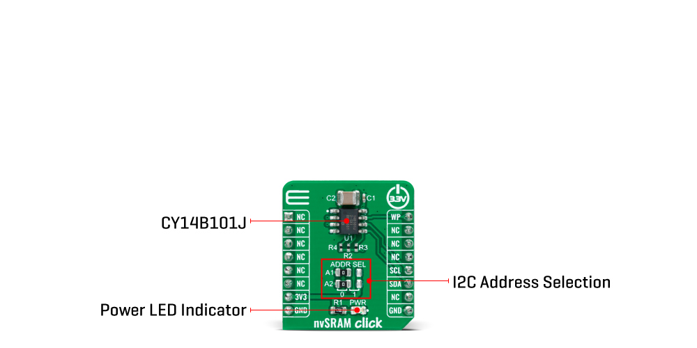
The nvSRAM Click Board™ is a compact add-on board that contains the most reliable nonvolatile memory. This board features the CY14B101J, a 1-Mbit nvSRAM organized as 128K words of 8 bits each with a nonvolatile element in each memory cell from Cypress Semiconductor. The embedded nonvolatile elements incorporate the QuantumTrap technology and provide highly reliable nonvolatile storage of data. Data transfer, initiated by the user through I2C commands, from SRAM to the nonvolatile elements takes place automatically at Power-Down. On the other hand, during the Power-Up, data is restored to the SRAM from the nonvolatile memory. This Click Board™ is suitable for all applications that require fast access and high reliability of stored data, and unlimited endurance.
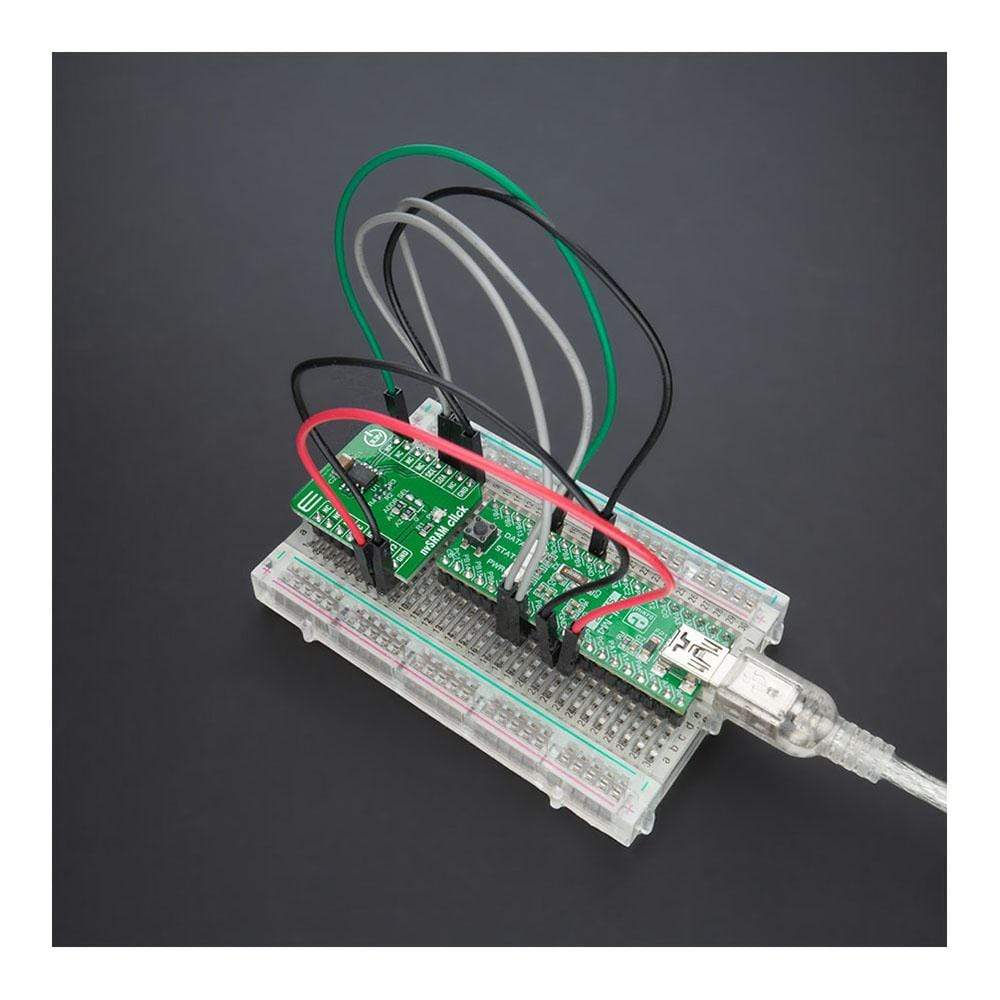
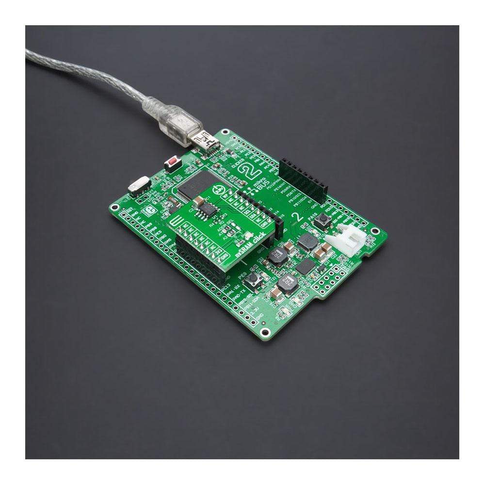
nvSRAM Click is supported by a mikroSDK compliant library, which includes functions that simplify software development. This Click Board™ comes as a fully tested product, ready to be used on a system equipped with the mikroBUS™ socket.
Downloads
How Does The nvSRAM Click Board™ Work?
The nvSRAM Click Board™ is based on the CY14B101J, a 1-Mbit nvSRAM organized as 128K words of 8 bits each with a nonvolatile element in each memory cell from Cypress Semiconductor. The CY14B101J integrates an SRAM cell and a nonvolatile memory cell into a single nvSRAM cell. In the Normal mode, all reads and writes happen directly from and to the SRAM portion of the nvSRAM. This provides faster write and read access compared to any existing nonvolatile memory technology such as EEPROM and Flash.
The nvSRAM specifies one million endurance cycles for nonvolatile cells with data retention of a minimum of 20 years. In the event of system power loss, data from the SRAM is transferred to its nonvolatile cell automatically by using energy stored in a capacitor labeled as C2. During the Power-Up, data from the nonvolatile cell is recalled automatically in the SRAM array and available to the user. The endurance cycle is consumed only when data transfer happens from the SRAM cells to nonvolatile cells during the Power-Down.
nvSRAM Click communicates with MCU using the standard I2C 2-Wire interface with a clock frequency up to 100kHz in the Standard, up to 400kHz in the Fast, up to 1MHz in the FastPlus, and up to 3.4MHz in the High-Speed Mode. The CY14B101J offers zero cycle delay write operation with infinite SRAM write endurance. Besides, it also allows the choice of the least significant bit (LSB) of its I2C slave address by positioning SMD jumpers labeled as ADDR SEL to an appropriate position marked as 0 and 1.
An additional feature of this Click board™ represents the configurable Write Protection function labeled as WP routed on the PWM pin of the mikroBUS™ socket. The WP pin is an active-high pin that protects the entire memory and all registers from write operations. This pin must be held high to inhibit all the write operations. When this pin is high, all memory and register writes are prohibited, and the address counter is not incremented.
This Click board™ is designed to be operated only with a 3.3V logic voltage level. A proper logic voltage level conversion should be performed before the Click board™ is used with MCUs with different logic levels.
SPECIFICATIONS
| Type | SRAM |
| Applications | Can be used for all applications that require fast access and high reliability of stored data, and unlimited endurance. |
| On-board modules | nvSRAM Click is based on the CY14B101J, a 1-Mbit nvSRAM organized as 128K words of 8 bits each with a nonvolatile element in each memory cell from Cypress Semiconductor. |
| Key Features | Low power consumption, 1-Mbit nonvolatile static random access memory, high reliability, high speed interface, write protection feature, and more. |
| Interface | I2C |
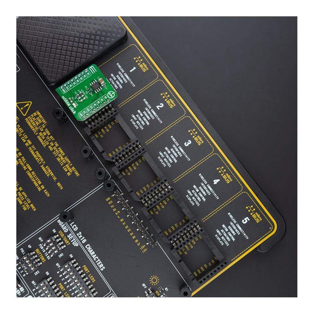
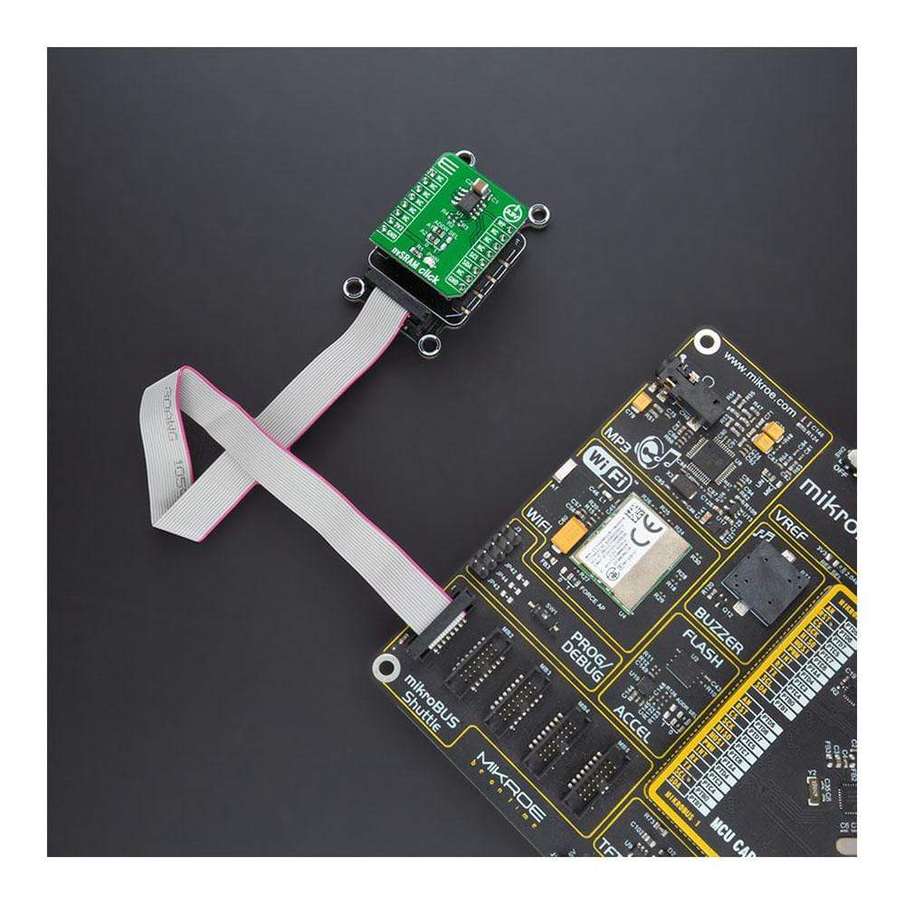
| Compatibility | mikroBUS |
| Click board size | S (28.6 x 25.4 mm) |
| Input Voltage | 3.3V |
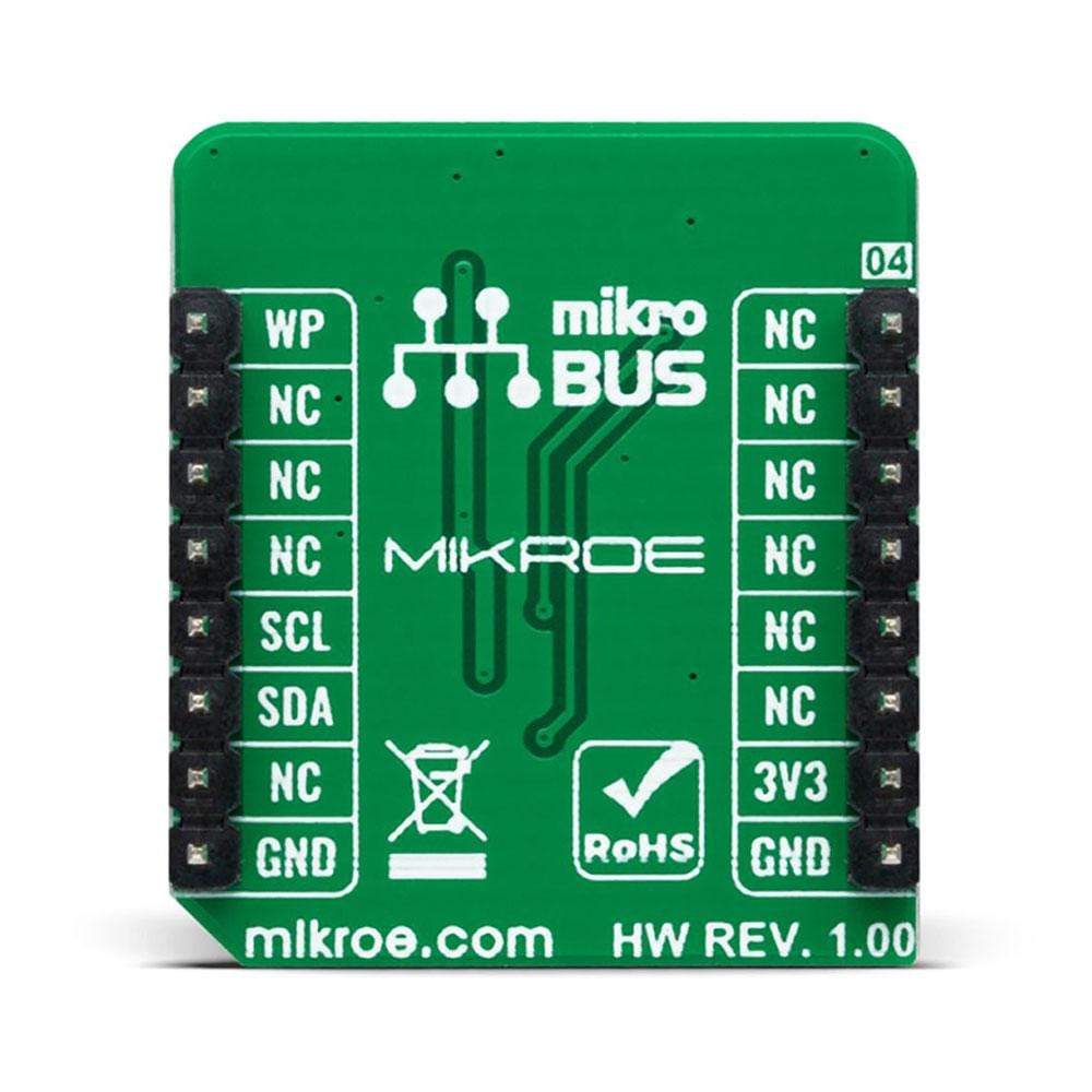
PINOUT DIAGRAM
This table shows how the pinout on nvSRAM Click corresponds to the pinout on the mikroBUS™ socket (the latter shown in the two middle columns).
| Notes | Pin | Pin | Notes | ||||
|---|---|---|---|---|---|---|---|
| NC | 1 | AN | PWM | 16 | WP | Write Protection | |
| NC | 2 | RST | INT | 15 | NC | ||
| NC | 3 | CS | RX | 14 | NC | ||
| NC | 4 | SCK | TX | 13 | NC | ||
| NC | 5 | MISO | SCL | 12 | SCL | I2C Clock | |
| NC | 6 | MOSI | SDA | 11 | SDA | I2C Data | |
| Power Supply | 3.3V | 7 | 3.3V | 5V | 10 | NC | |
| Ground | GND | 8 | GND | GND | 9 | GND | Ground |
ONBOARD SETTINGS AND INDICATORS
| Label | Name | Default | Description |
|---|---|---|---|
| LD1 | PWR | - | Power LED Indicator |
| JP1-JP2 | ADDR SEL | Left | I2C Address Selection: Left position 0, Right position 1 |
NVSRAM CLICK ELECTRICAL SPECIFICATIONS
| Description | Min | Typ | Max | Unit |
|---|---|---|---|---|
| Supply Voltage | -0.5 | 3.3 | 4.1 | V |
| Memory Size | - | - | 1 | Mbit |
| nvSRAM Write Endurance | 1.000.000 | - | - | Write Cycles |
| nvSRAM Data Retention | 20 | - | - | Years |
| Operating Temperature Range | -40 | - | +85 | °C |
| General Information | |
|---|---|
Part Number (SKU) |
MIKROE-4441
|
Manufacturer |
|
| Physical and Mechanical | |
Weight |
0.016 kg
|
| Other | |
EAN |
8606027381355
|
Frequently Asked Questions
Have a Question?
Be the first to ask a question about this.