


Mikroelektronika d.o.o.
SRAM 3 Click Board™
SRAM 3 Click Board™
SKU: MIKROE-4293
Couldn't load pickup availability
Overview
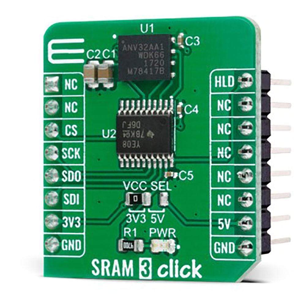
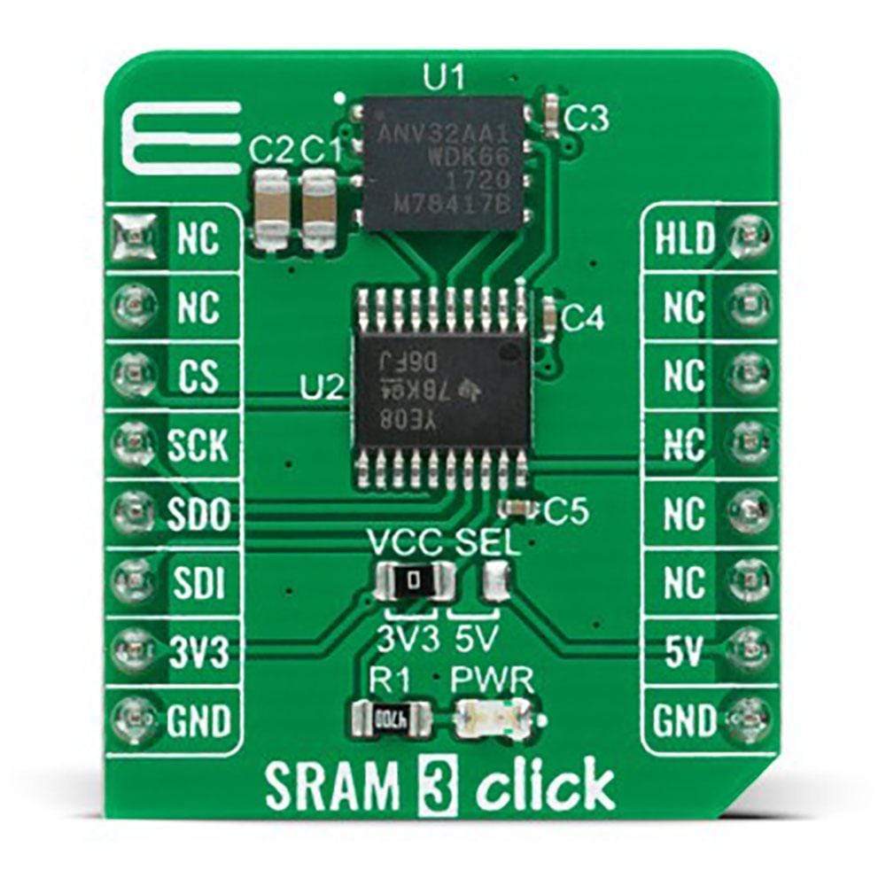
The SRAM 3 Click Board™ is a 1 Mb Serial Random Access Memory add-on board with the non-volatile SONOS storage element included with each memory cell, organized as 128k words of 8 bits each. This board features the ANV32AA1WDK66 an SRAM memory from Anvo-System Dresden. The device is accessed by a high-speed SPI-compatible bus. The serial SRAM provides fast access & cycle times, ease of use and unlimited read & write endurance of a standard SRAM. With dedicated safety features like supporting high data accuracy and all other features makes SRAM 3 Click excellent choice to store drive profiles, configurations and similar data, which are typically stored in a FLASH.
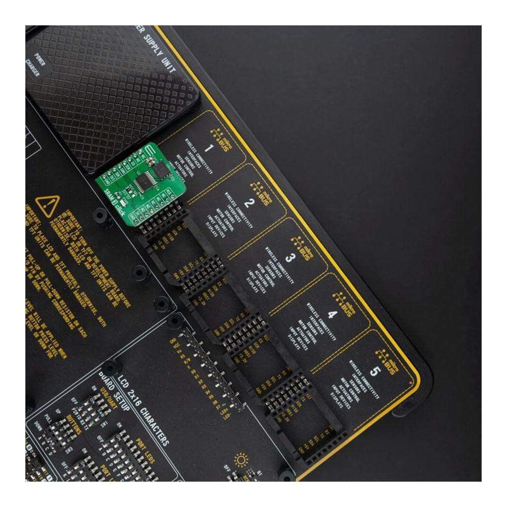
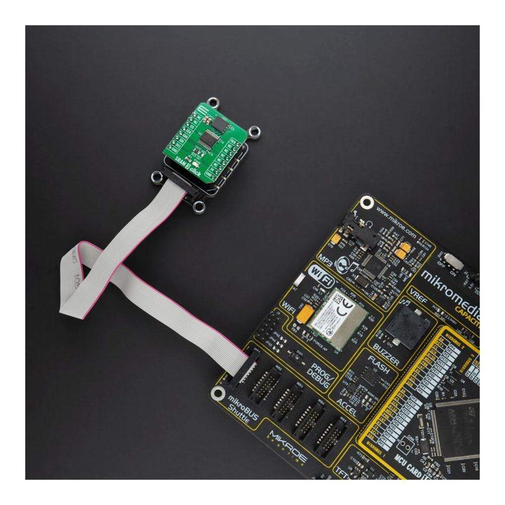
The SRAM 3 Click Board™ is supported by a mikroSDK compliant library, which includes functions that simplify software development. This Click Board™ comes as a fully tested product, ready to be used on a system equipped with the mikroBUS™ socket.
Downloads
How Does The SRAM 3 Click Board™ Work?
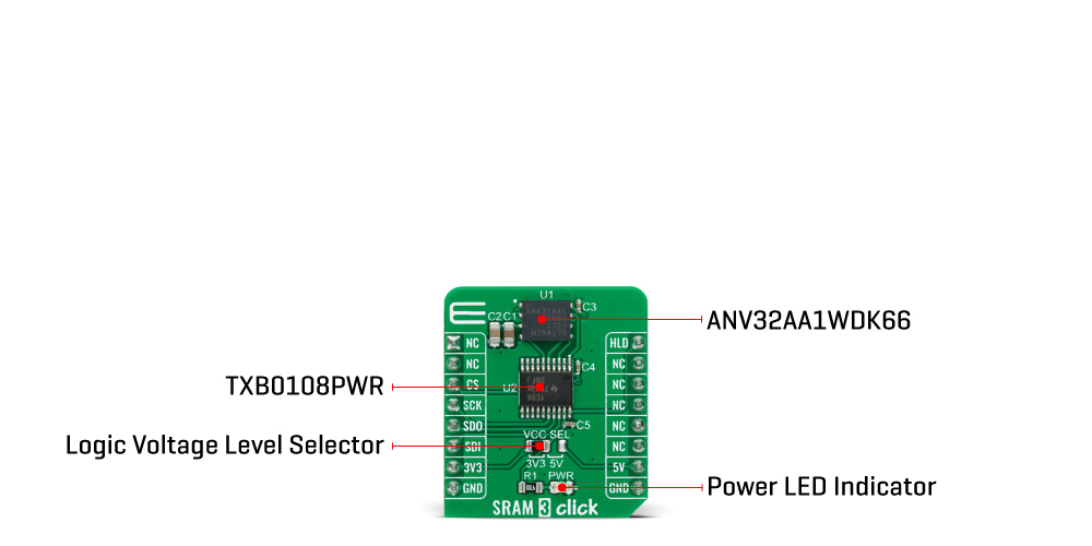
The SRAM 3 Click Board™ is based on the ANV32AA1WDK66, a serial non-volatile SRAM with double memory architecture and SPI serial interface organized as 128k words of 8 bits each from Anvo-System Dresden. This memory has a silicon-oxide-nitride-oxide-silicon (SONOS) flash storage element included with each memory cell. In the case of an unforeseeable operating voltage drop below a defined value, the SONOS technology enables non-volatile storage of all data in less than 15ms. An integrated Power Down functionality of the SRAM 3 Click with a standby current of less than 1µA ensures its low power consumption, with recovery time from Power-Down Mode of typically of 60µs.
This ANV32AA1WDK66 possesses unique safety features, such as Checksum Protected Memory Accesses (Secure READ and Secure WRITE instructions) and Time Monitoring that ensures a high degree of reliability of this Click board™. Corrupt data cannot overwrite existing memory content, and even valid data would not overwrite on a corrupted address. The SRAM 3 Click also provides some distinctive advantages of SRAMs, such as fast access times and unlimited write/read endurance.
The SRAM 3 Click Board™ incorporates an additional IC, labelled as the TXB0108PWR, an 8-bit bidirectional voltage level translator from Texas Instruments. This allows the Click board™ to be used with a much extensive range of MCUs. At the same time, the TXB0108PWR protects the ANV32AA1WDK66 from the Electrostatic Discharges (ESD) up to ±15 kV, making SRAM 3 Click a very reliable embedded storage solution.
The ANV32AA1WDK66 communicates with MCU using the standard SPI serial interface that supports modes 0 and 3 with a maximum frequency of 66 MHz. It also possesses additional HOLD function routed at the PWM pin of the mikroBUS™ socket labelled as HLD. This pin is used in conjunction with the CS pin to select the device. When the device is selected, and a serial sequence is underway, an HLD pin can be used to pause the serial communication with the master device without resetting the serial sequence.
The SRAM 3 Click Board™ is designed to be operated with both 3.3V and 5V logic levels that can be selected via VCC SEL jumper. This allows for both 3.3V and 5V capable MCUs to use the SPI communication lines properly. However, the Click board™ comes equipped with a library that contains easy to use functions and an example code that can be used as a reference for further development.
SPECIFICATIONS
| Type | SRAM |
| Applications | The SRAM 3 Click Board™ can be used to store drive profiles, configurations, and similar data, or for applications such as medical devices, industrial automation (for example, motor control and robotics), smart metering systems, and many others. |
| On-board modules | SRAM 3 Click is based on the ANV32AA1WDK66, a serial non-volatile SRAM with double memory architecture and SPI serial interface organized as 128k words of 8 bits each from Anvo-System Dresden. |
| Key Features | Low power consumption, high storage capacity, fast access & cycle times, high data accuracy, ease of use, and unlimited read & write accessed by a high-speed SPI compatible bus, and more. |
| Interface | SPI |
| Compatibility | mikroBUS |
| Click board size | S (28.6 x 25.4 mm) |
| Input Voltage | 3.3V or 5V |
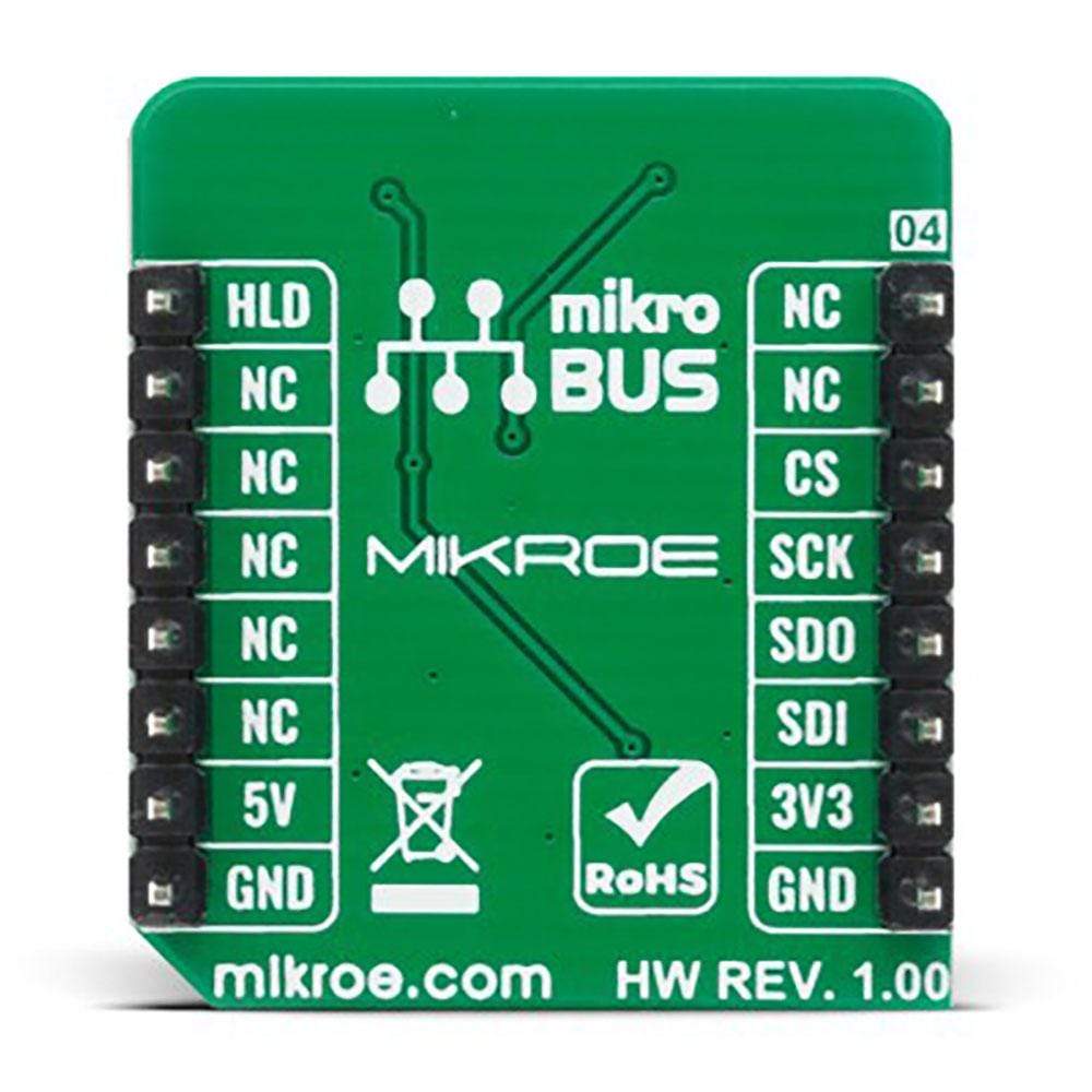
PINOUT DIAGRAM
This table shows how the pinout of the SRAM 3 Click Board™ corresponds to the pinout on the mikroBUS™ socket (the latter shown in the two middle columns).
| Notes | Pin | Pin | Notes | ||||
|---|---|---|---|---|---|---|---|
| NC | 1 | AN | PWM | 16 | HLD | HOLD | |
| NC | 2 | RST | INT | 15 | NC | ||
| SPI Chip Select | CS | 3 | CS | RX | 14 | NC | |
| SPI Clock | SCK | 4 | SCK | TX | 13 | NC | |
| SPI Data OUT | SDO | 5 | MISO | SCL | 12 | NC | |
| SPI Data IN | SDI | 6 | MOSI | SDA | 11 | NC | |
| Power Supply | 3.3V | 7 | 3.3V | 5V | 10 | 5V | Power Supply |
| Ground | GND | 8 | GND | GND | 9 | GND | Ground |
ONBOARD SETTINGS AND INDICATORS
| Label | Name | Default | Description |
|---|---|---|---|
| LD1 | PWR | - | Power LED Indicator |
| JP1 | VCC SEL | Left | Power Supply Voltage Selection 3V3/5V, left position 3v3, right position 5v |
SRAM 3 CLICK ELECTRICAL SPECIFICATIONS
| Description | Min | Typ | Max | Unit |
|---|---|---|---|---|
| Supply Voltage | 2.7 | 3.3 | 3.6 | V |
| Average VCC Current at 66MHz | - | - | 5 | mA |
| Operating Temperature Range | 0 | 25 | 70 | °C |
| General Information | |
|---|---|
Part Number (SKU) |
MIKROE-4293
|
Manufacturer |
|
| Physical and Mechanical | |
Weight |
0.017 kg
|
| Other | |
EAN |
8606027380709
|
Frequently Asked Questions
Have a Question?
Be the first to ask a question about this.