


Mikroelektronika d.o.o.
6LoWPAN T Click Board™
6LoWPAN T Click Board™
SKU: MIKROE-2218
Couldn't load pickup availability


Overview
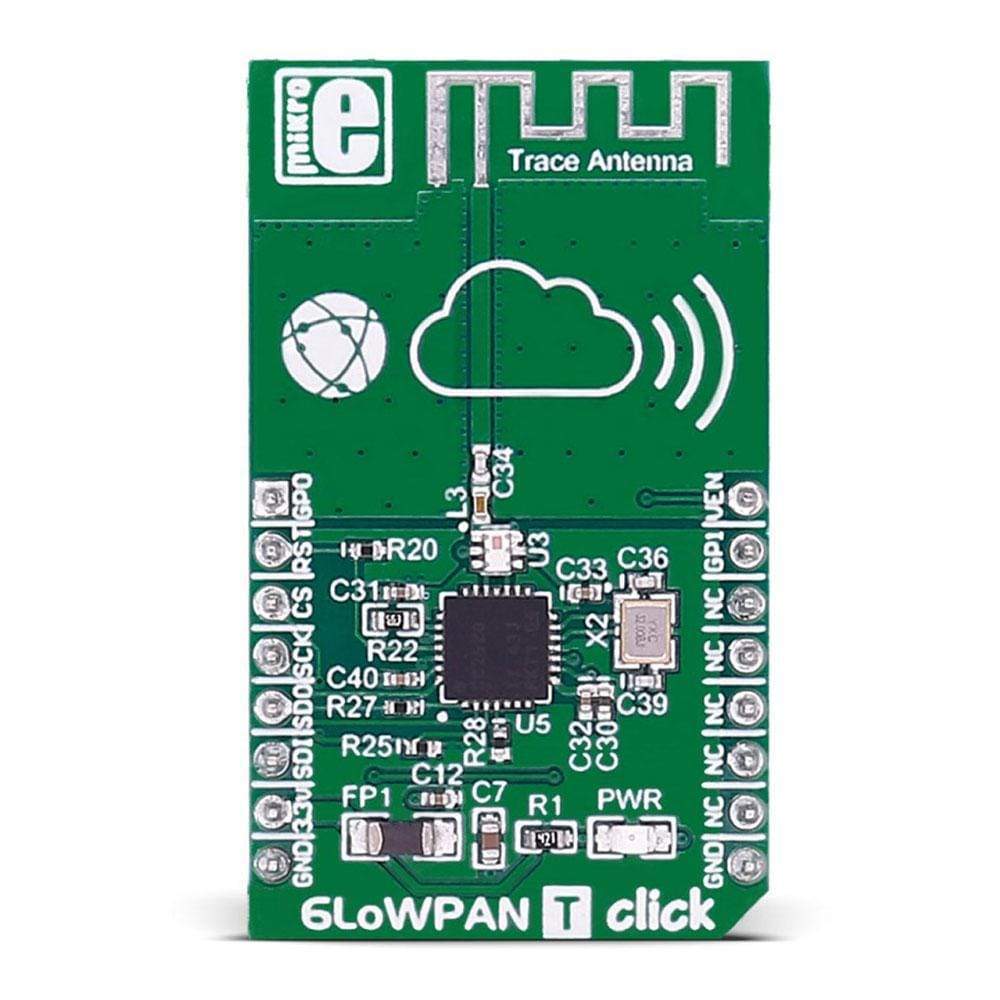
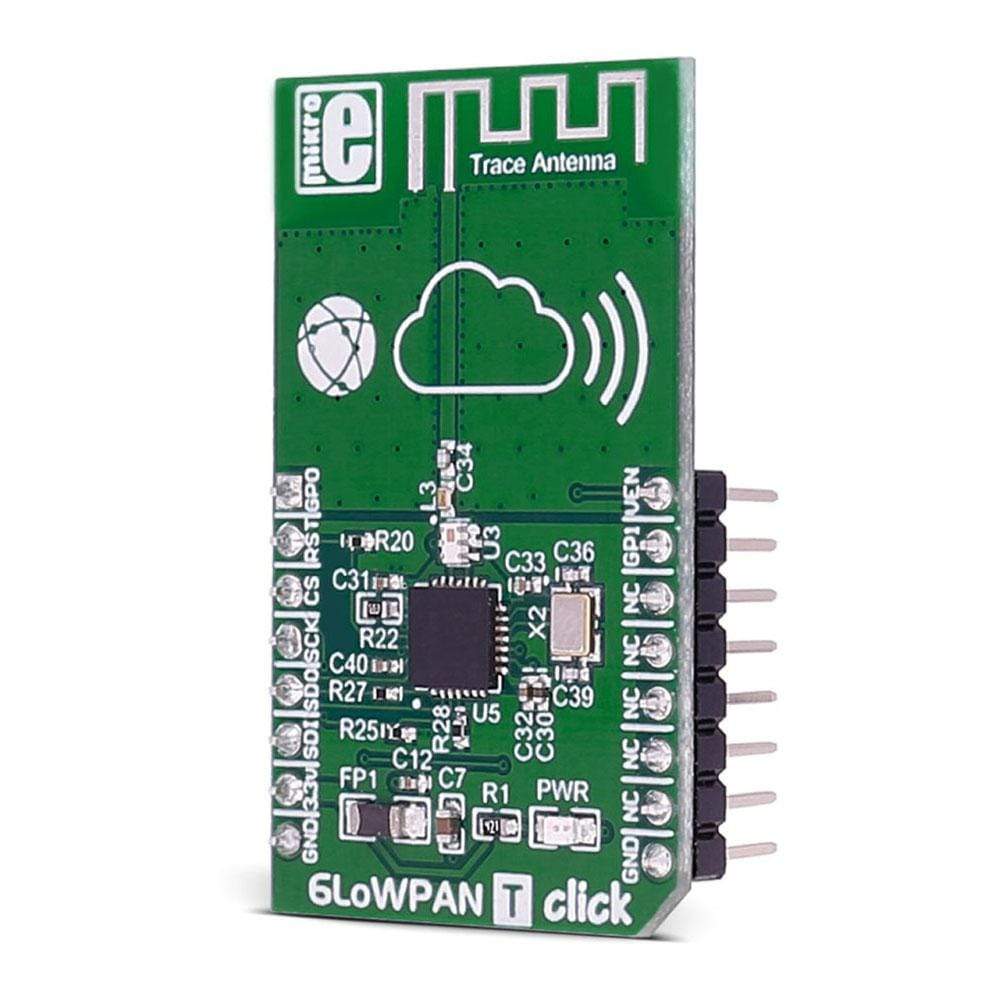
The 6LoWPAN T Click Board™ carries the CC2520 2.4GHz RF transceiver.
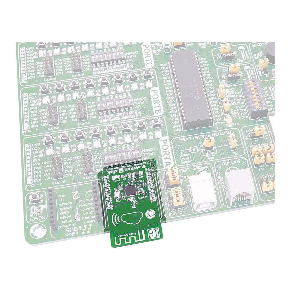
The 6LoWPAN T Click Board™ is designed to run on a 3.3V power supply. It communicates with the target microcontroller over SPI interface, with additional functionality provided by the following pins on the MikroBUS line: PWM, INT, RST, AN.
Downloads
The 6LoWPAN T Click Board™ is based on the CC2520 2.4GHz RF transceiver. The click is designed to run on a 3.3V power supply. It communicates with the target microcontroller over SPI interface, with additional functionality provided by the following pins on the mikroBUS™ line: PWM, INT, RST, AN.
CC2520 Features
The CC2520 is TI's second-generation ZigBee®/IEEE 802.15.4 RF transceiver for the 2.4GHz unlicensed ISM band. This chip enables industrial grade applications by offering state-of-the-art selectivity/co-existence, excellent link budget, operation up to 125°C and low voltage operation.
In addition, the CC2520 provides extensive hardware support for frame handling, data buffering, burst transmissions, data encryption, data authentication, clear channel assessment, link quality indication and frame timing information.
SPECIFICATIONS
| Type | 6LoWPAN |
| Applications | IEEE 802.15.4 systems, ZigBee® systems, industrial monitoring and control, home and building automation, Automatic Meter Reading, Low-power wireless sensor networks, etc. |
| On-board modules | CC2520 is TI's second-generation ZigBee®/IEEE 802.15.4 RF transceiver |
| Key Features | Selectivity/co-existence, excellent link budget, operation up to 125°C and low voltage operation |
| Interface | GPIO,SPI |
| Compatibility | mikroBUS |
| Click board size | M (42.9 x 25.4 mm) |
| Input Voltage | 3.3V |
PINOUT DIAGRAM
This table shows how the pinout of the 6LoWPAN T Click Board™ corresponds to the pinout on the mikroBUS™ socket (the latter shown in the two middle columns).
| Notes | Pin | Pin | Notes | ||||
|---|---|---|---|---|---|---|---|
| General purpose digital I/O | RF GPIO0 | 1 | AN | PWM | 16 | RF VREG EN | When high, digital voltage regulator is active |
| External reset pin, active low | RF RST# | 2 | RST | INT | 15 | RF GPIO 1 | General purpose digital I/O |
| Chip select | RF CS | 3 | CS | TX | 14 | NC | |
| Serial clock | RF SCK | 4 | SCK | RX | 13 | NC | |
| Master input slave output | RF MISO | 5 | MISO | SCL | 12 | NC | |
| Master output slave input | RF MOSI | 6 | MOSI | SDA | 11 | NC | |
| Power supply | +3.3V | 7 | 3.3V | 5V | 10 | NC | |
| Ground | GND | 8 | GND | GND | 9 | GND | Ground |
| General Information | |
|---|---|
Part Number (SKU) |
MIKROE-2218
|
Manufacturer |
|
| Physical and Mechanical | |
Weight |
0.018 kg
|
| Other | |
EAN |
8606018710904
|
Frequently Asked Questions
Have a Question?
Be the first to ask a question about this.