


Mikroelektronika d.o.o.
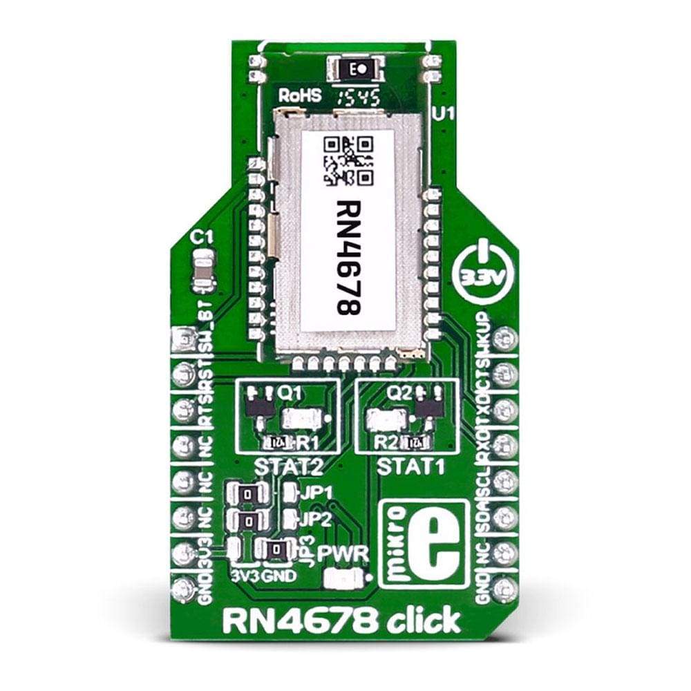
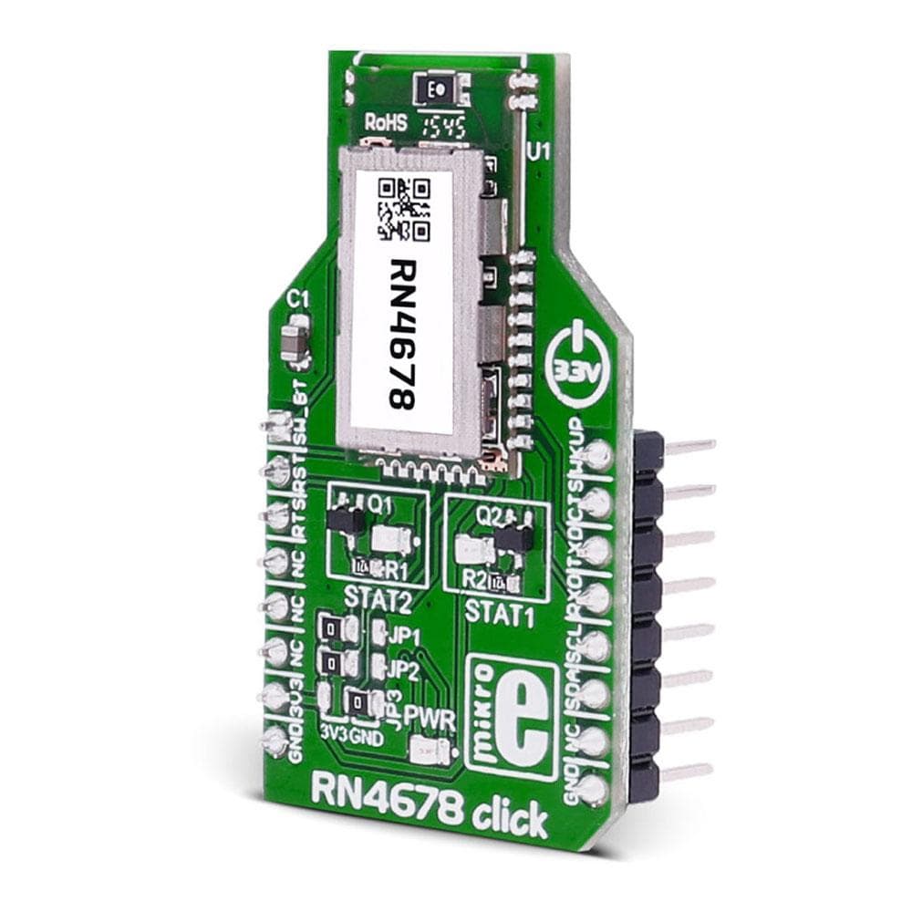
RN4678 Click Board™
RN4678 Click Board™
SKU: MIKROE-2545
Couldn't load pickup availability

Overview
The RN4678 Click Board™ is based on Microchip's RN4678 Bluetooth® 4.2 dual mode module.
The RN4678 Click Board™ is designed to run on a 3.3V power supply. It communicates with the target microcontroller over I2C and UART interface, with additional functionality provided by the following pins on the mikroBUS™ line: AN, RST, CS, PWM, INT.
Downloads
RN4678 MODULE FEATURES
The RN4678 from Microchip is a fully certified, Bluetooth version 4.2 module. Use it to add Bluetooth wireless capability to your project.
The module includes an on-board Bluetooth stack, power management subsystem, 2.4 GHz transceiver, and RF power amplifier.
Data transfer is achieved through the Bluetooth link by sending or receiving data through SPP in Bluetooth (BT) Classic mode and through Transparent UART in the BLE mode.
The RN4678 contains an integral ceramic chip antenna.
STRONG ENCRYPTION
The RN4678 module has strong AES128 Encryption. A 128-bit encryption is one of the most powerfull encryption algorithms. AES stands for Advanced Encryption Standard and it is a symmetric encryption algorithm.
SPECIFICATIONS
| Type | BT/BLE |
| Applications | Internet of Things (IoT), secure payment, home and security, health and fitness, industrial and data logger, LED lighting, etc. |
| On-board modules | RN4678 module from Microchip |
| Key Features | Frequency: 2.402 GHz to 2.480 GHz, RX Sensitivity: -90 dBm (BR/EDR), -92 dBm (LE), Bluetooth SIG 4.2 Qualified |
| Interface | I2C,GPIO,UART |
| Compatibility | mikroBUS |
| Click Board™ size | M (42.9 x 25.4 mm) |
| Input Voltage | 3.3V |
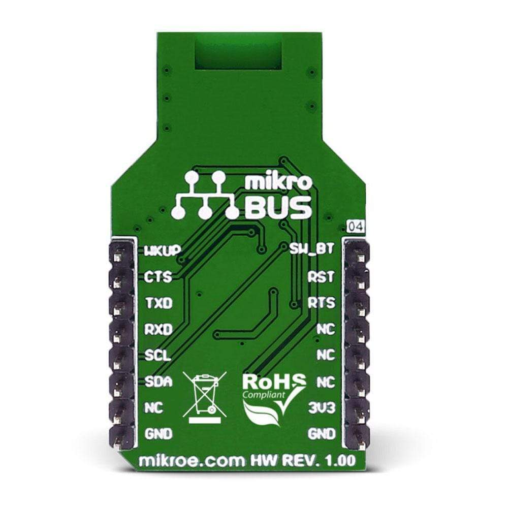
PINOUT DIAGRAM
This table shows how the pinout on RN4678 Click Board™ corresponds to the pinout on the mikroBUS socket (the latter shown in the two middle columns).
| Notes | Pin | Pin | Notes | ||||
|---|---|---|---|---|---|---|---|
| Software Button | SW_BTN | 1 | AN | PWM | 16 | WKUP | Wake-up from Sleep mode |
| Module Reset (internal pull-up). Apply a pulse of at least 63 ns. | RST_N | 2 | RST | INT | 15 | CTS | Clear To Send |
| Configurable Control or Indication pin or UART RTS (output) | RTS | 3 | CS | TX | 14 | TXD | UART data output |
| NC | 4 | SCK | RX | 13 | RXD | UART data input | |
| NC | 5 | MISO | SCL | 12 | SCL | I2C Clock | |
| NC | 6 | MOSI | SDA | 11 | SDA | I2C Data | |
| Power supply | +3.3V | 7 | 3.3V | 5V | 10 | NC | |
| Ground | GND | 8 | GND | GND | 9 | GND | Ground |
JUMPERS AND SETTINGS
| Designator | Name | Default Position | Default Option | Description |
|---|---|---|---|---|
| JP1 | P2_0 | Left | HIGH | System configuration pin - Along with P2_4 and EAN pins, used to set the module in any of the following three modes: Application mode (for normal operation), Test mode (to change EEPROM values), and Write Flash mode (to enter the new firmware into the module); |
| JP2 | P2_4 | Left | HIGH | System configuration pin - Along with P2_0 and EAN pins, used to set the module in any of the following three modes: Application mode (for normal operation), Test mode (to change EEPROM values), and Write Flash mode (to enter new firmware into the module); |
| JP3 | EAN | Right | LOW | External address-bus negative pin. System configuration pin along with P2_0 and P2_4 pins, used to set the module in any of the following three modes: Application mode (for normal operation), Test mode (to change EEPROM values), and Write Flash mode (to enter new firmware into the module); |
| General Information | |
|---|---|
Part Number (SKU) |
MIKROE-2545
|
Manufacturer |
|
| Physical and Mechanical | |
Weight |
0.019 kg
|
| Other | |
EAN |
8606018710423
|
Frequently Asked Questions
Have a Question?
Be the first to ask a question about this.