


Mikroelektronika d.o.o.
PWM 2 Click Board™
PWM 2 Click Board™
SKU: MIKROE-3148
Couldn't load pickup availability
Overview
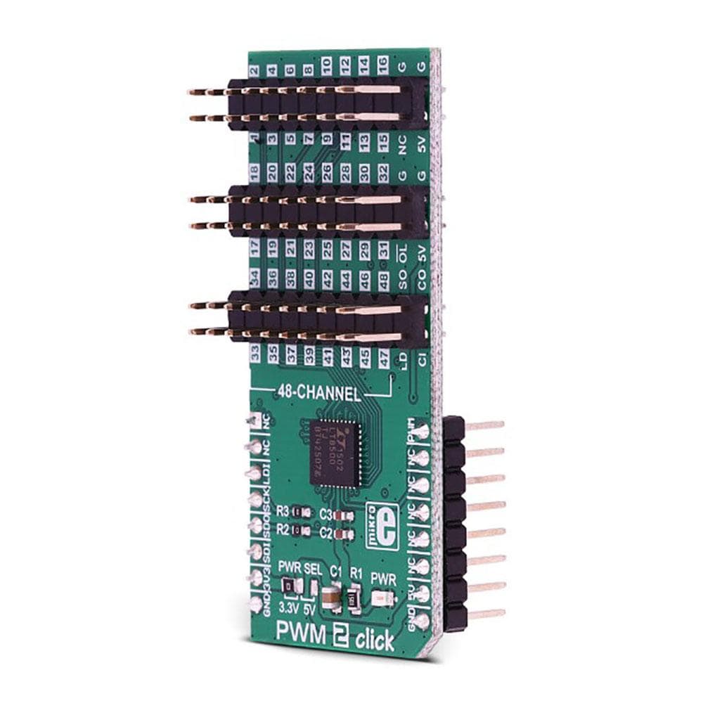
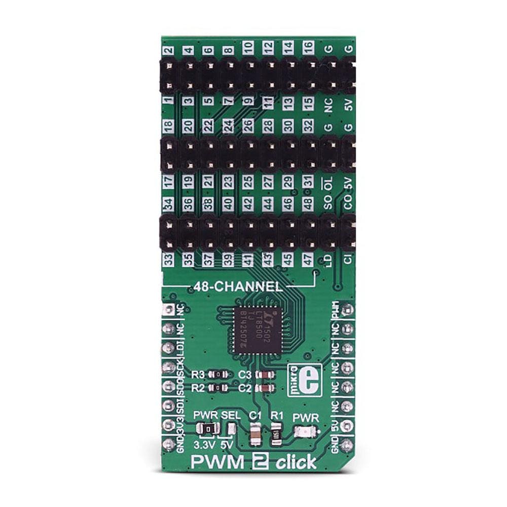
The PWM 2 Click Board™ offers 48 independently controlled PWM channels, available over the on-board headers, perfectly suited for driving LEDs. Each channel has a 12-bit PWM register associated to it, with the addition of the 6-bit correction register, also known as the dot correction register. PWM 2 is able to detect both synchronization errors and open LED errors, signaling the error via the dedicated pin and the status frame.
The PWM 2 Click Board™ fully supports cascading, exposing all the necessary pins on the on-board headers, so it can support a large array of LED elements.
Downloads
The possibility to cascade more devices, as well as the ability to additionally fine-tune each PWM channel separately, compensating the brightness differences between the LED elements (dots), make PWM 2 click an ideal solution for building both small-scale and large-scale LED matrices and displays. Although it is targeted toward driving LEDs, the PWM 2 Click Board™ can also be used for other purposes, such as the motor control, industrial control, robotics, and similar applications that can benefit from having compact 48 channel PWM driver.
How Does The PWM 2 Click Board™ Work?
The main component of the PWM 2 Click Board™ is the LT8500, a 48-Channel LED PWM generator with 12-Bit resolution and 50MHz serial interface, from Analog Devices. This IC has 48 independent 12-bit PWM channels, each with 6-bit correction up to 50% of the original duty cycle. The LT8500 IC is clocked by a clock signal at the PWMCK pin. The frequency of the clock signal can go up to 25MHz, generating the PWM output frequency of up to 6.1kHz, which is sufficient for most purposes. The maximum speed of the LT8500 serial interface goes up to 50MHz in theory, but in practice, it will depend on many factors.
The clock signal at the PWM pin of the mikroBUS™ is triggering an internal counter register (PWMCK). This register is compared with the content of the PWMRSYNC register, associated with each channel. Whenever the counter value is less than the value written in a specific channel PWMRSYNC register, the PWM output of that channel goes to a HIGH logic level. The frequency of the output PWM signal is therefore determined by the frequency the clock signal at the PWMCK pin. This represents the basic operating principle of the LTC8500 IC. The PWMCK pin is routed to the PWM pin of the mikroBUS™.
The device uses an industry-standard SPI interface for the communication. The LDI pin acts as the normal Chip Select, latching the SPI data in, but it has an additional function if held to a HIGH logic level for more than 50µs. In that case, the IC will be reset, and all outputs will be blanked. Therefore, care should be taken not to hold this pin to a HIGH logic level, for more than 5µs. The LDI pin is routed to the CS pin of the mikroBUS™ and it is labeled as LDI.
Besides the usual SPI interface lines, the LT8500 PWM generator IC provides a serial interface clock output signal (SCKO), allowing additional devices to be connected in the parallel 5-wire topology (LDI, SCKI, SDI, SDO, and SCKO). This allows large-scale cascading, without the need for the skew balancing or buffering the signals. These additional pins are available at the standard 2.54 pitch headers on board. These additional pins on the header are described in a table, below. More information about cascading and using the SCKO feature of the IC can be found in the LT8500 datasheet.
The device is controlled by sending commands via the SPI interface, embedded in a command frame. There are eight different commands which are used to control the following parameters: PWM outputs update (synchronously or asynchronously to PWM period), the dot correction factor, self-test initialization, phase shifting between banks (groups of 16 channels), enabling/ disabling of the PWM output drivers, and enabling/disabling of the dot correction . A frame consists of a 12-bit data field for each of the 48 PWM channels, followed by an 8-bit command field, which contains one of the eight command codes. The status frame is clocked on the SDO pin, providing the host MCU with the frame information: LED fault status, phase shifting status, correction status, synchronization status, and so on. This information can be used either for troubleshooting or for other purposes by the host MCU application.
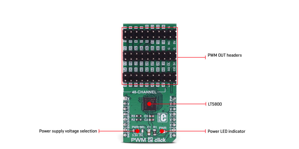
As already mentioned, additional functionalities of the LT8500 IC are offered via the onboard headers, along with the 48 PWM channel outputs. The outputs are not meant to drive devices with high current, so PWM 2 click is best used as the driver for additional circuitry, whether it is a simple MOSFET LED driver, or a more complex ICs, such as the LT3595A LED driver, for which a special input pin is reserved, allowing open LED conditions to be detected, even on the externally connected LT3595 IC. Onboard headers also offer fixed 5V output from the mikroBUS™ for the auxiliary purposes.
The PWM 2 Click Board™ offers an operating voltage level selection between 3.3V and 5V by switching an SMD jumper labeled as the PWR SEL to an appropriate position. This allows both 3.3V and 5V MCUs to be interfaced with this Click board™.
SPECIFICATIONS
| Type | PWM |
| Applications | The PWM 2 Click Board™ can be used for driving up to 48 independent channels with the PWM signal of the programmable duty cycle, and can be used for driving LED matrices and displays, but it can also be used for the motor control, industrial control, robotics, and similar applications |
| On-board modules | LT8500, a 48-Channel LED PWM generator with 12-Bit resolution and 50MHz serial interface, from Linear Technology division of Analog Devices |
| Key Features | A complete pinout required for cascading available on the 2.54mm pin headers, along with the 48 independent PWM channels, each with programmable duty cycle, dot brightness correction for brightness uniformity, and error reporting for open LED via the status frame response |
| Interface | PWM,SPI |
| Compatibility | mikroBUS |
| Click board size | L (57.15 x 25.4 mm) |
| Input Voltage | 3.3V or 5V |
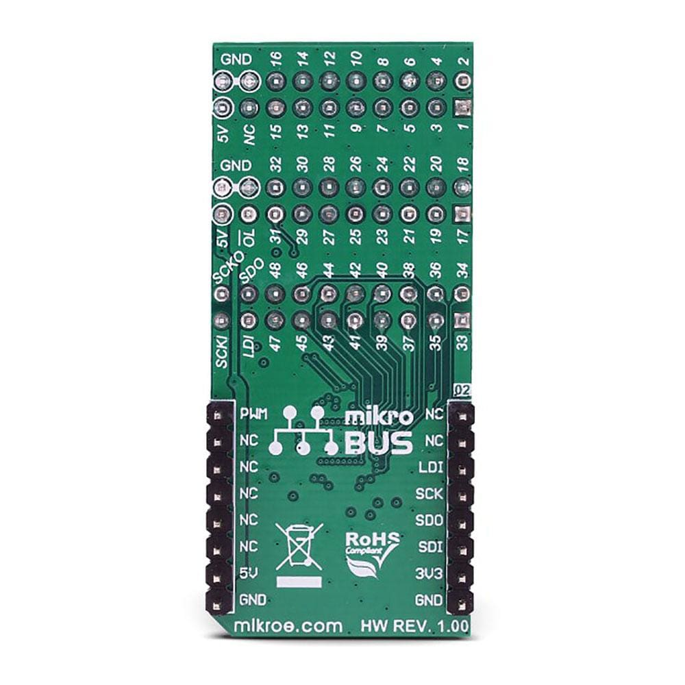
PINOUT DIAGRAM
This table shows how the pinout on the PWM 2 Click Board™ corresponds to the pinout on the mikroBUS™ socket (the latter shown in the two middle columns).
| Notes | Pin | Pin | Notes | ||||
|---|---|---|---|---|---|---|---|
| NC | 1 | AN | PWM | 16 | PWM | Clock Signal IN | |
| NC | 2 | RST | INT | 15 | NC | ||
| Latch Data In/Blank | LDI | 3 | CS | RX | 14 | NC | |
| SPI clock | SCK | 4 | SCK | TX | 13 | NC | |
| SPI Data OUT | SDO | 5 | MISO | SCL | 12 | NC | |
| SPI Data IN | SDI | 6 | MOSI | SDA | 11 | NC | |
| Power supply | 3.3V | 7 | 3.3V | 5V | 10 | 5V | Power supply |
| Ground | GND | 8 | GND | GND | 9 | GND | Ground |
ONBOARD JUMPERS AND SETTINGS
| Label | Name | Default | Description |
|---|---|---|---|
| LD1 | PWR | - | Power LED indicator |
| J1 | PWR SEL | Right | Power Supply voltage selection: left position 3.3V, right position 5V |
ONBOARD CONNECTORS
| Label | Description |
|---|---|
| 1 - 48 | Channel 1 to Channel 48 PWM outputs |
| LD | Latch Data In/Blank pin (shared with the mikroBUS™) |
| SO | SPI Serial Data Out (shared with the mikroBUS™) |
| C | SPI Serial Clock In (shared with the mikroBUS™) |
| CO | SPI Serial Clock Out |
| OL | #OPENLED pin used to detect an external open LED condition |
| 5V | 5V power supply from the mikroBUS™ power rail |
| GND | Ground |
| General Information | |
|---|---|
Part Number (SKU) |
MIKROE-3148
|
Manufacturer |
|
| Physical and Mechanical | |
Weight |
0.03 kg
|
| Other | |
EAN |
8606018713493
|
Frequently Asked Questions
Have a Question?
Be the first to ask a question about this.