


Mikroelektronika d.o.o.
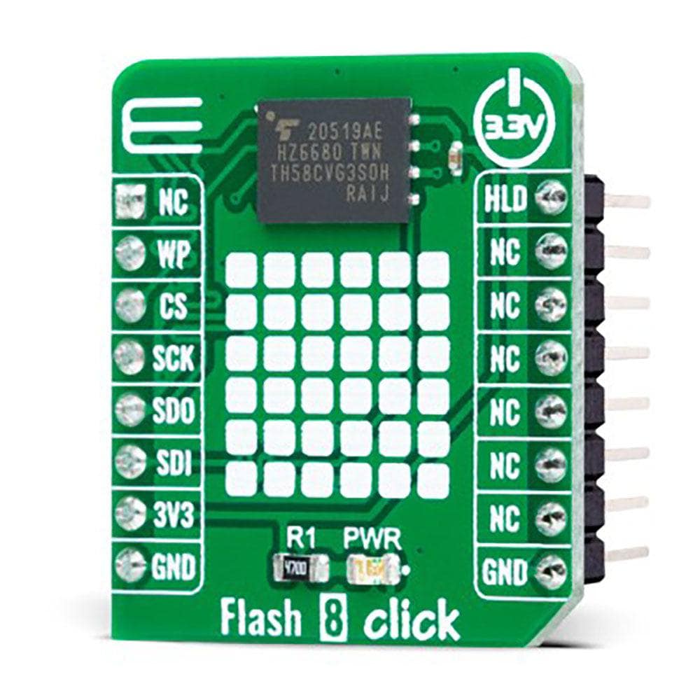
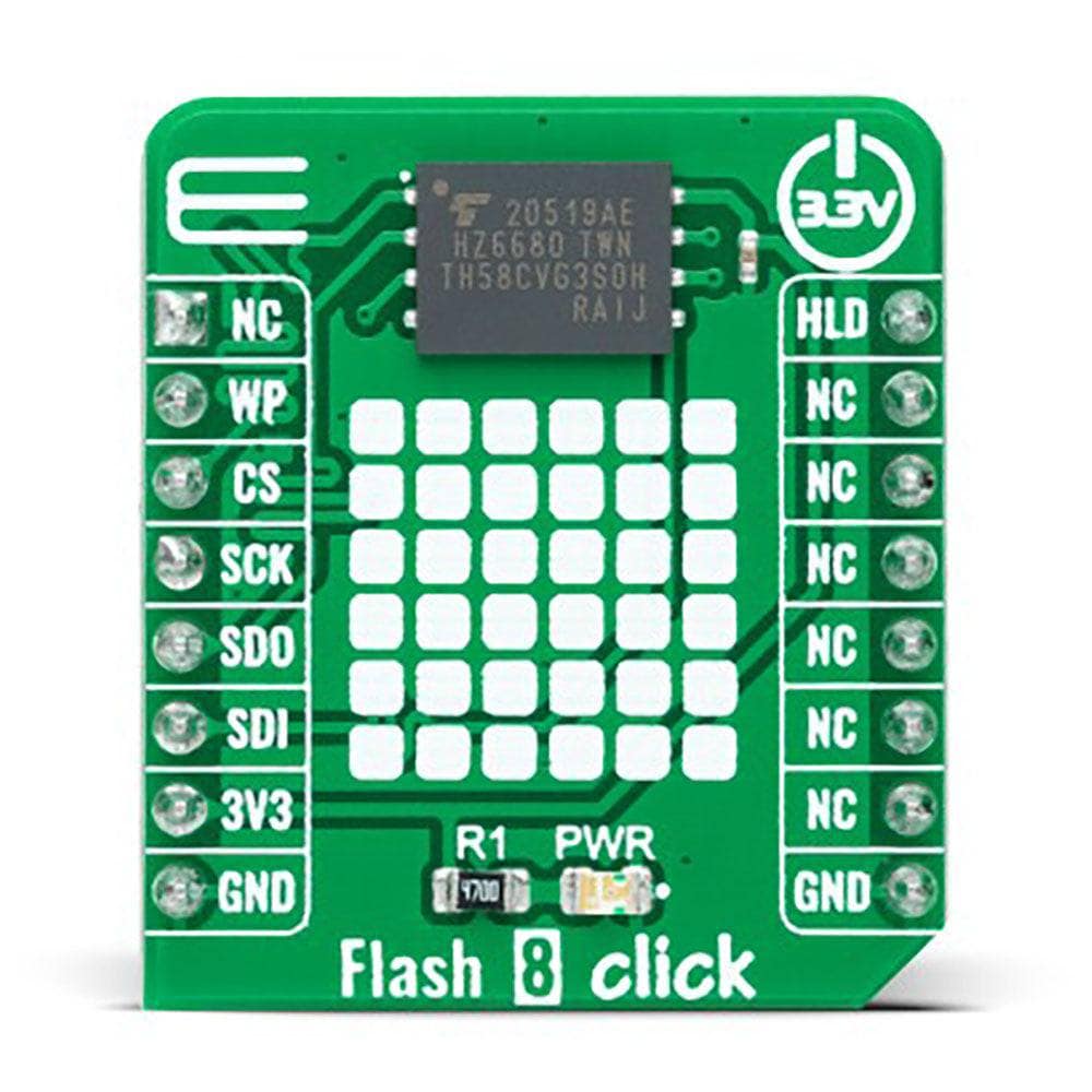
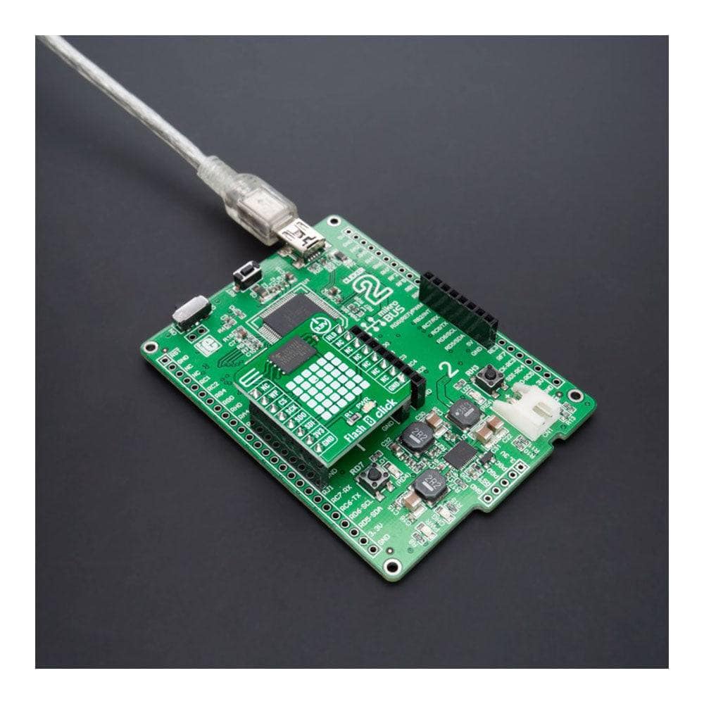
Flash 8 Click Board™
Flash 8 Click Board™
SKU: MIKROE-5293
Couldn't load pickup availability


Key Features
Overview
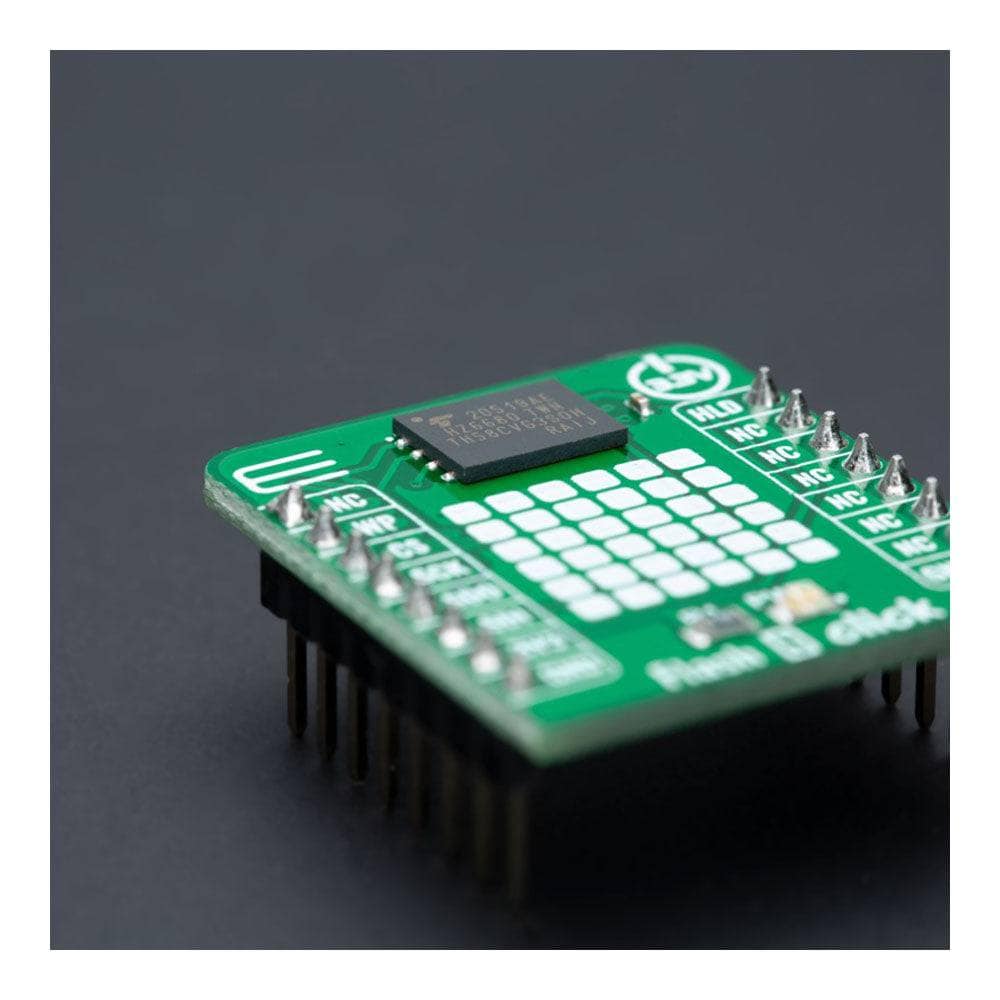
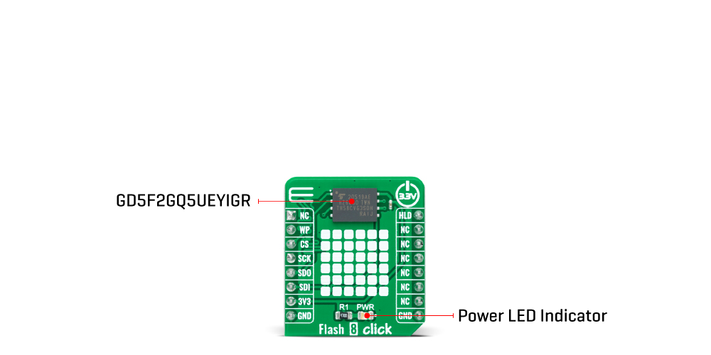
The Flash 8 Click Board™ is a compact add-on board representing a highly reliable memory solution. This board features the GD5F2GQ5UEYIGR, a 2Gb high-density non-volatile memory storage solution for embedded systems from GigaDevice Semiconductor. It is based on an industry-standard NAND Flash memory core, representing an attractive alternative to SPI-NOR and standard parallel NAND Flash with advanced features. The GD5F2GQ5UEYIGR also has advanced security features (8K-Byte OTP region), software/hardware write protection, can withstand many write cycles (minimum 100k), and has a data retention period greater than ten years. This Click board™ is suitable for storage and data transfer in consumer devices and industrial applications.
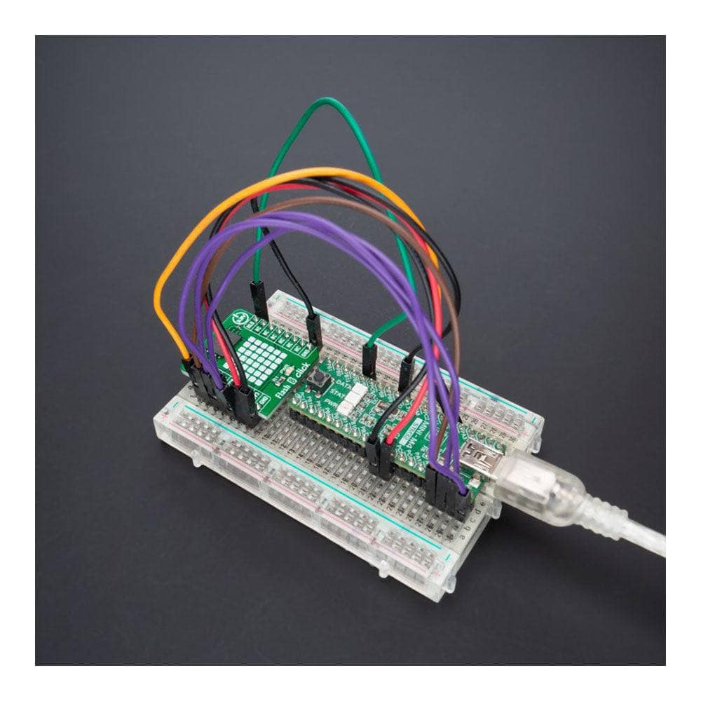
The Flash 8 Click Board™ is supported by a mikroSDK compliant library, which includes functions that simplify software development. This Click board™ comes as a thoroughly tested product, ready to be used on a system equipped with the mikroBUS™ socket.
Downloads
How Does The Flash 8 Click Board™ Work?
The Flash 8 Click Board™ is based on the GD5F2GQ5UEYIGR, a highly reliable serial Flash memory solution offering flexibility designed for use in a wide variety of consumer applications from GigaDevice Semiconductor. It comes with a density of 2Gb based on an industry-standard NAND Flash memory core, representing an attractive alternative to SPI-NOR and standard parallel NAND Flash with advanced features. Organized as 256Mx8, the GD5F2GQ5UEYIGR has advanced security features (8K-Byte OTP region). It specifies a minimum of 100.000 endurance cycles with data retention of 10 years, allowing it to handle unlimited reads/writes to the memory.
The Flash 8 Click Board™ communicates with MCU through an industry-standard SPI interface (Dual and QSPI compatible) that enables high clock speed, supporting the two most common SPI modes, SPI Mode 0 and 3, with a maximum frequency of 104MHz. It is programmed/read in page-based operations and erased in block-based operations. Data is transferred to/from the NAND Flash memory array, page by page, to a data register and a cache register which is closest to I/O control circuits, acting as a data buffer for the I/O data (enable page and random data READ/WRITE and copy back operations). In addition to the SPI communication, this Click board™ also has two additional pins used for Write Protection and HOLD function routed to the RST and PWM pins of the mikroBUS™ socket.
The configurable Write Protection, marked as WP and routed on the RST pin of the mikroBUS™ socket, prevents the block lock bits from being overwritten and must be held low to inhibit all the write operations to registers. When this pin is low, also by setting the appropriate bits, all memory and register write are prohibited, and the address counter is not incremented. On the other hand, the HOLD pin labelled as HLD and routed to the PWM pin of the mikroBUS™ socket stops any serial communications with the device. Still, it doesn't stop the operation of reading programming or erasing in progress.
The Flash 8 Click Board™ can be operated only with a 3.3V logic voltage level. The board must perform appropriate logic voltage level conversion before using MCUs with different logic levels. What should be paid special attention to is the fact that if power shortage or power failure happens before Write/Erase operation is complete, it will cause loss or damage to data. However, the Click board™ comes equipped with a library containing functions and an example code that can be used, as a reference, for further development.
SPECIFICATIONS
| Type | FLASH |
| Applications | Can be used for storage and data transfer in consumer devices and industrial applications |
| On-board modules | GD5F2GQ5UEYIGR - serial Flash memory solution from GigaDevice Semiconductor |
| Key Features | 2Gb NAND flash, Standard/Dual/Quad SPI, high speed clock frequency, protection features, reliability, enhanced access performance, low power consumption, and more |
| Interface | QSPI,SPI |
| Compatibility | mikroBUS |
| Click board size | S (28.6 x 25.4 mm) |
| Input Voltage | 3.3V |
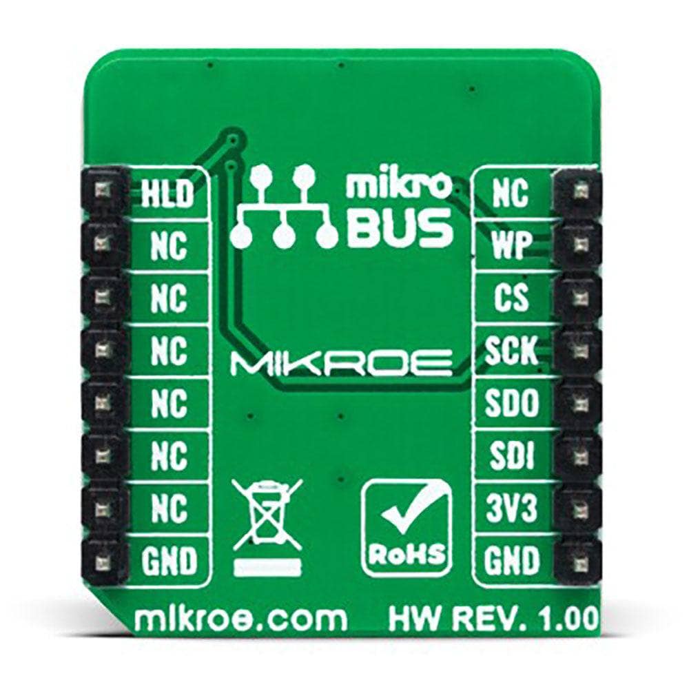
PINOUT DIAGRAM
This table shows how the Flash 8 Click Board™ corresponds to the pinout on the mikroBUS™ socket (the latter shown in the two middle columns).
| Notes | Pin | Pin | Notes | ||||
|---|---|---|---|---|---|---|---|
| NC | 1 | AN | PWM | 16 | HLD | QSPI IO3 / SPI Suspension | |
| QSPI IO2 / Write Protection | WP | 2 | RST | INT | 15 | NC | |
| SPI Chip Select | CS | 3 | CS | RX | 14 | NC | |
| SPI Clock | SCK | 4 | SCK | TX | 13 | NC | |
| SPI Data OUT | SDO | 5 | MISO | SCL | 12 | NC | |
| SPI Data IN | SDI | 6 | MOSI | SDA | 11 | NC | |
| Power Supply | 3.3V | 7 | 3.3V | 5V | 10 | NC | |
| Ground | GND | 8 | GND | GND | 9 | GND | Ground |
ONBOARD SETTINGS AND INDICATORS
| Label | Name | Default | Description |
|---|---|---|---|
| LD1 | PWR | - | Power LED Indicator |
FLASH 8 CLICK ELECTRICAL SPECIFICATIONS
| Description | Min | Typ | Max | Unit |
|---|---|---|---|---|
| Supply Voltage | - | 3.3 | - | V |
| Memory Size | - | - | 2 | Gb |
| Write Endurance | 100k | - | - | Cycles |
| Data Retention | 10 | - | - | Years |
| Operating Temperature Range | -40 | +25 | +85 | °C |
| General Information | |
|---|---|
Part Number (SKU) |
MIKROE-5293
|
Manufacturer |
|
| Physical and Mechanical | |
Weight |
0.02 kg
|
| Other | |
EAN |
8606027387890
|
Frequently Asked Questions
Have a Question?
Be the first to ask a question about this.