


Mikroelektronika d.o.o.
I2C MUX 2 Click Board™
I2C MUX 2 Click Board™
SKU: MIKROE-4094
Couldn't load pickup availability


Overview
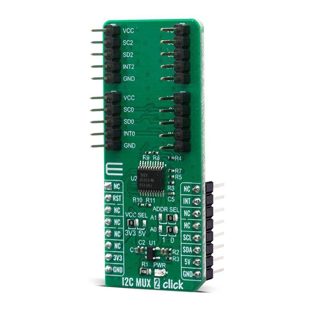
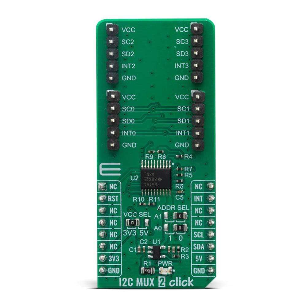
The I2C MUX 2 Click Board™ is a quad bidirectional translating I2C and SMBus switch with reset and interrupt functions, intended for applications with I2C slave address conflicts. It features a quad bidirectional translating switch controlled via the I2C bus, labelled as TCA9545A from Texas Instruments. Four interrupt inputs (INT3–INT0), one for each of the downstream pairs, are provided on the click board. One interrupt (INT) output acts as an AND of the four interrupt inputs. Click has two address jumpers, allowing up to four TCA9545A devices on the same bus. The I2C MUX 2 Click Board™ allows voltage translation between 1.8V, 2.5V, 3.3V, and 5V buses, and also supports hot insertion. The TCA9546A can work on a 0 - 400 kHz clock frequency range and is ideal for communication with numerous devices that share the identical slave address on the same bus.
The I2C MUX 2 Click Board™ is supported by a mikroSDK compliant library, which includes functions that simplify software development. This Click Board™ comes as a fully tested product, ready to be used on a system equipped with the mikroBUS™ socket.
Downloads
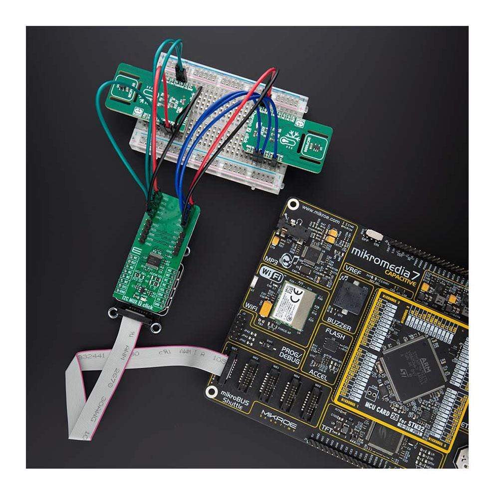
How Does The I2C MUX 2 Click Board™ Work?
The I2C MUX 2 Click Board™ uses the TCA9545A, a 4-channel, bidirectional translating I2C switch. The master SCL/SDA signal pair is directed to four channels of slave devices, SC0/SD0-SC3/SD3. Any individual downstream channel can be selected as well as any combination of the four channels. The TCA9545A also supports interrupt signals in order for the master to detect an interrupt on the INT output terminal that can result from any of the slave devices connected to the INT3-INT0 input terminals. The device offers an active-low RESET input which resets the state machine and allows the TCA9545A to recover should one of the downstream I2C buses get stuck in a low state. The state machine of the device can also be reset by cycling the power supply, VCC, also known as a power-on reset (POR). Both the RESET function and a POR will cause all channels to be deselected.
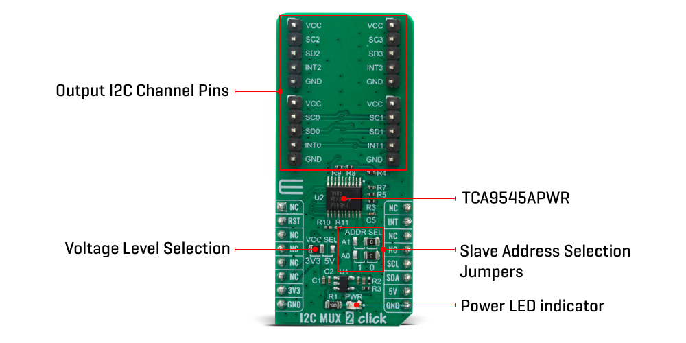
The connections of the I2C data path are controlled by the same I2C master device that is switched to communicate with multiple I2C slaves. The I2C slave address can be configured by soldering SMD jumpers labelled as ADDR SEL to set the least significant bit (LSB). After the successful acknowledgment of the slave address, a single 8-bit control register is written to or read from to determine the selected channels and state of the interrupts. The TCA9545A may also be used for voltage translation, allowing the use of different bus voltages on each SCn/SDn pair such that 1.8-V, 2.5-V, or 3.3-V parts can communicate with 5-V parts. This is achieved by using external pull-up resistors to pull the bus up to the desired voltage for the master and each slave channel.
One or several SCn/SDn downstream pairs, or channels, are selected by the contents of the control register. After the TCA9545A has been addressed, the control register is written. The four LSBs of the control byte are used to determine which channel or channels are to be selected. When a channel is selected, it becomes active after a stop condition has been placed on the I2C bus. This ensures that all SCn/SDn lines are in a high state when the channel is made active so that no false conditions are generated at the time of connection. A stop condition must occur always right after the acknowledge cycle.
The TCA9545A provides four interrupt inputs (one for each channel) and one open-drain interrupt output. When an interrupt is generated by any device, it is detected by the TCA9545A and the interrupt output is driven low. The channel does not need to be active for the detection of the interrupt. A bit also is set in the control register. Bits 4–7 of the control register correspond to channels 0–3 of the TCA9545A, respectively. Therefore, if an interrupt is generated by any device connected to channel 1, the state of the interrupt inputs is loaded into the control register when a read is accomplished. Likewise, an interrupt on any device connected to channel 0 would cause bit 4 of the control register to be set on the read. The master then can address the TCA9545A and read the contents of the control register to determine which channel contains the device generating the interrupt. The master then can reconfigure the TCA9545A to select this channel and locate the device generating the interrupt and clear it. It should be noted that more than one device can provide an interrupt on a channel, so it is up to the master to ensure that all devices on a channel are interrogated for an interrupt. The interrupt inputs can be used as general-purpose inputs if the interrupt function is not required. If unused, interrupt input(s) must be connected to VCC.
The I2C MUX 2 Click Board™ can be supplied and interfaced with both 3.3V and 5V without the need for any external components. The onboard SMD jumper labelled as VCC SEL allows voltage selection for interfacing with both 3.3V and 5V microcontrollers.
SPECIFICATIONS
| Type | I2C |
| Applications | Servers, Routers (telecom switching equipment), Factory automation, Products with I2C slave address conflicts (multiple, identical temp sensors) |
| On-board modules | The I2C MUX 2 Click Board™ uses the TCA9545A IC, a quad bidirectional translating switch, from Texas Instruments |
| Key Features | The 1-of-4 Bidirectional translating switches, Allows voltage-level translation between 1.8-V, 2.5-V, 3.3-V, and 5-V buses |
| Interface | I2C |
| Compatibility | mikroBUS |
| Click board size | L (57.15 x 25.4 mm) |
| Input Voltage | 3.3V,5V |
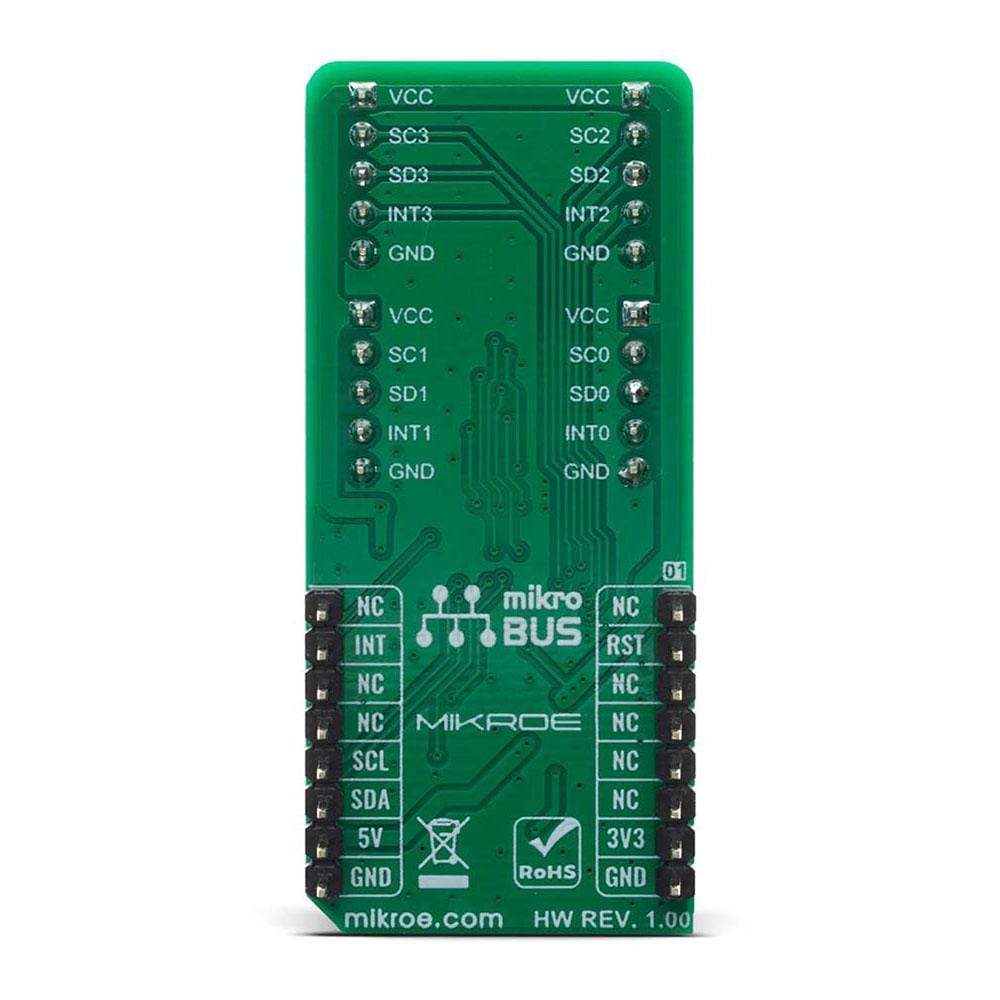
PINOUT DIAGRAM
This table shows how the pinout of the I2C MUX 2 Click Board™ corresponds to the pinout on the mikroBUS™ socket (the latter shown in the two middle columns).
| Notes | Pin | Pin | Notes | ||||
|---|---|---|---|---|---|---|---|
| NC | 1 | AN | PWM | 16 | NC | ||
| Reset | RTS | 2 | RST | INT | 15 | INT | Interrupt |
| NC | 3 | CS | RX | 14 | NC | ||
| NC | 4 | SCK | TX | 13 | NC | ||
| NC | 5 | MISO | SCL | 12 | SCL | I2C Clock | |
| NC | 6 | MOSI | SDA | 11 | SDA | I2C Data | |
| Power Supply | 3.3V | 7 | 3.3V | 5V | 10 | 5V | Power Supply |
| Ground | GND | 8 | GND | GND | 9 | GND | Ground |
ONBOARD SETTINGS AND INDICATORS
| Label | Name | Default | Description |
|---|---|---|---|
| LD1 | PWR | - | Power LED Indicator |
| JP1 | VCC SEL | Left | Power Supply Voltage Selection 3V3/5V, left position 3v3, right position 5v |
| JP2-3 | ADDR SEL | Right | Slave address LSB selection: left position 1, right position 0 |
| General Information | |
|---|---|
Part Number (SKU) |
MIKROE-4094
|
Manufacturer |
|
| Physical and Mechanical | |
Weight |
0.021 kg
|
| Other | |
EAN |
8606018717347
|
Frequently Asked Questions
Have a Question?
Be the first to ask a question about this.