


Mikroelektronika d.o.o.
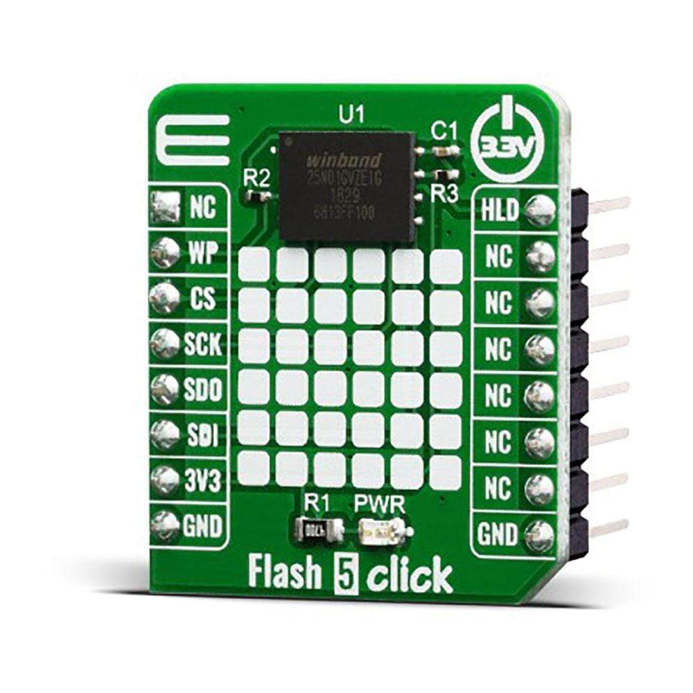
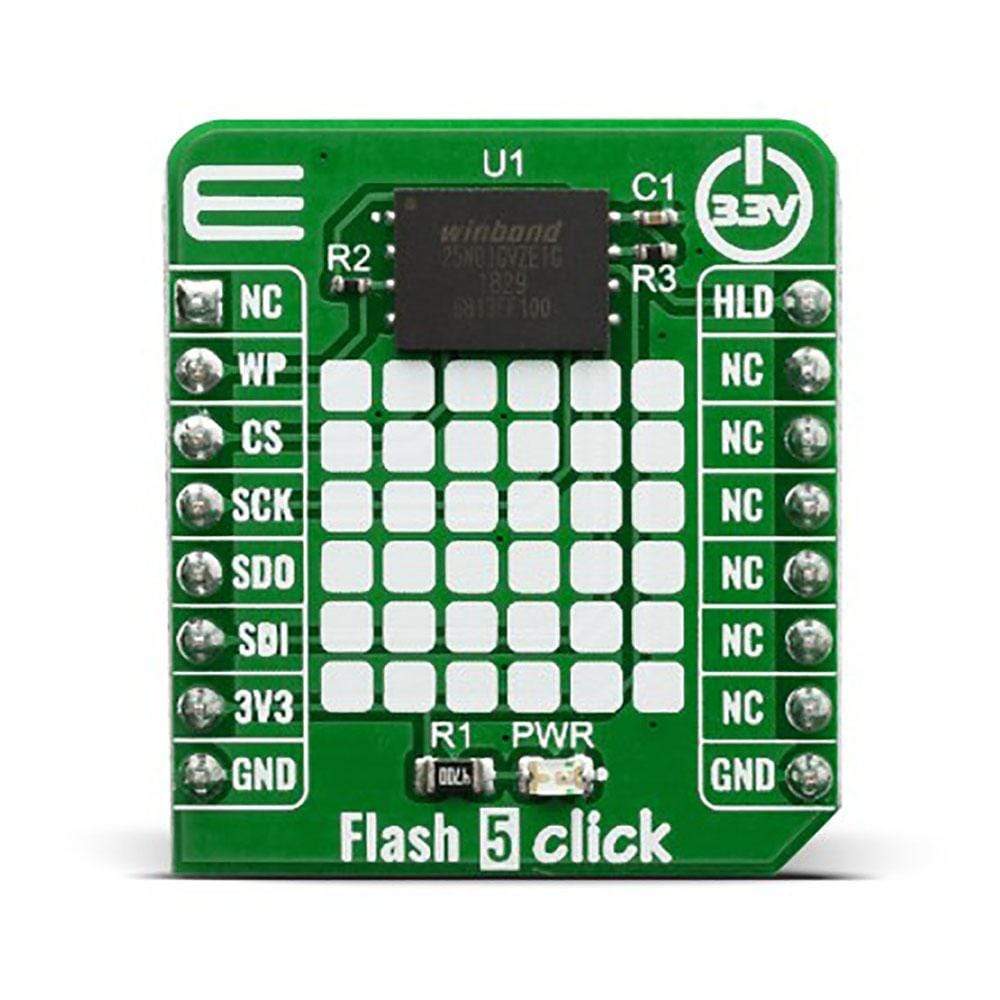
Flash 5 Click Board™
Flash 5 Click Board™
SKU: MIKROE-3780
Couldn't load pickup availability


Overview
The Flash 5 Click Board™ is a perfect solution for the mass storage option in various embedded applications. It features the W25N01GVZEIG/IT (1G-bit) Serial SLC NAND Flash Memory from Winbond which provides a storage solution for systems with limited space, pins and power. The W25N SpiFlash family incorporates the popular SPI interface and the traditional large NAND non-volatile memory space. They are ideal for code shadowing to RAM, executing code directly from Dual/Quad SPI (XIP) and storing voice, text and data.
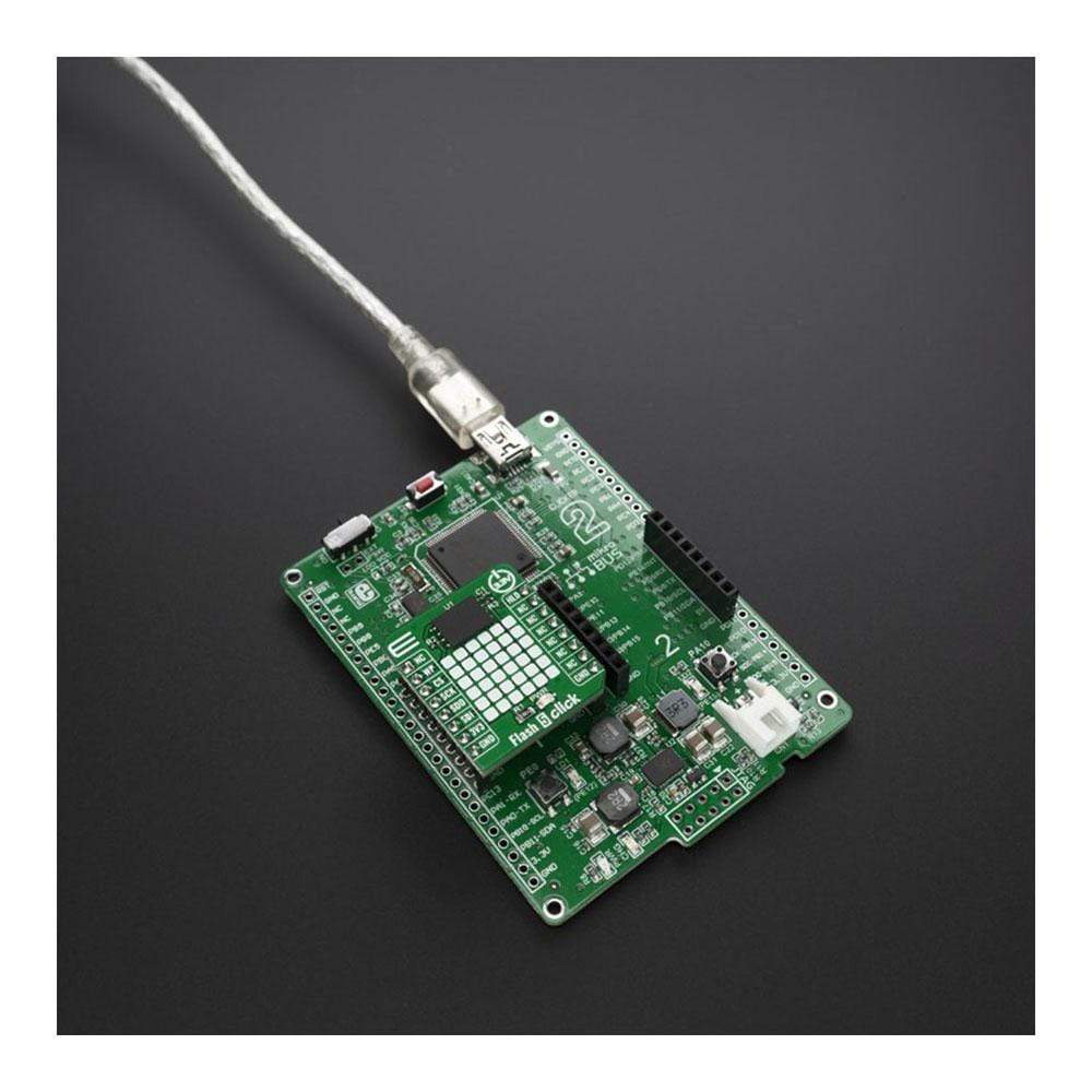
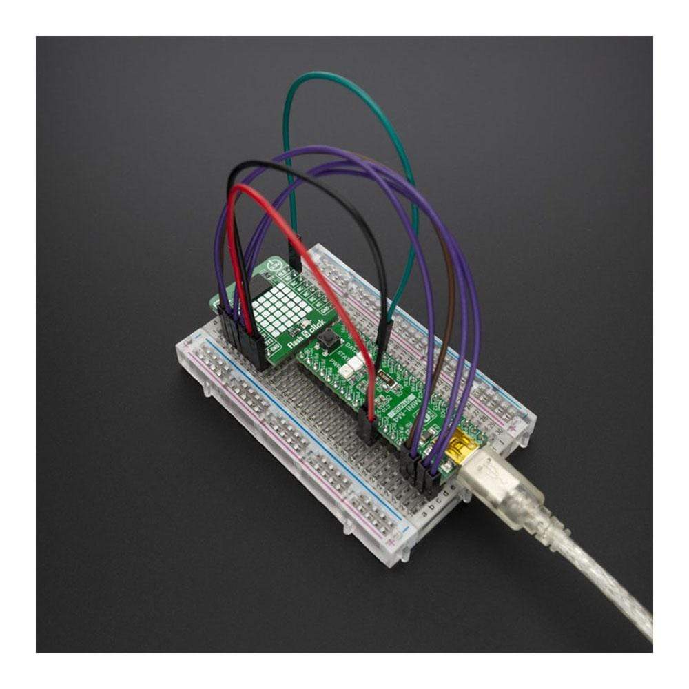
The Flash 5 Click Board™ is supported by a mikroSDK compliant library, which includes functions that simplify software development. This Click Board™ comes as a fully tested product, ready to be used on a system equipped with the mikroBUS™ socket.
Downloads
How Does The Flash 5 Click Board™ Work?
The Flash 5 Click Board™ is based on the W25N01GVZEIG/IT (1G-bit) Serial SLC NAND Flash Memory from Winbond. The device operates on a single 3.3V power supply with current consumption as low as 25mA active and 10µA for standby. All W25N SpiFlash family devices are offered in space-saving packages which were impossible to use in the past for the typical NAND flash memory.
The W25N01GVZEIG/IT 1G-bit memory array is organized into 65,536 programmable pages of 2,048-bytes each. The entire page can be programmed at one time using the data from the 2,048-Byte internal buffer. Pages can be erased in groups of 64 (128KB block erase). The W25N01GVZEIG/IT has 1,024 erasable blocks.
The Flash 5 Click Board™ uses the standard Serial Peripheral Interface (SPI), supporting SPI clock frequencies of up to 104MHz. Besides that, the W25N01GVZEIG/IT provides a new Continuous Read Mode that allows for efficient access to the entire memory array with a single Read command. This feature is ideal for code shadowing applications. Also, it offers the highest performance thanks to the Serial NAND Flash with 104MHz Standard/Dual/Quad SPI clocks and a 50MB/S continuous data transfer rate. Given the fact it has a efficient "Continuous Read Mode", it allows direct read access to the entire array. However, the performance also depends on the main MCU used with this Click board™.
A Hold pin, Write Protect pin and programmable write protection, provide further control flexibility. Additionally, the device supports JEDEC standard manufacturer and device ID, one 2,048-Byte Unique ID page, one 2,048-Byte parameter page and ten 2,048-Byte OTP pages. To provide better NAND flash memory manageability, user configurable internal ECC, bad block management are also available in W25N01GVZEIG/IT.
The W25N01GVZEIG/IT is accessed through an SPI compatible bus consisting of four signals: Serial Clock (CLK), Chip Select (/CS), Serial Data Input (DI) and Serial Data Output (DO). Standard SPI instructions use the DI input pin to serially write instructions, addresses or data to the device on the rising edge of CLK. The DO output pin is used to read data or status from the device on the falling edge of CLK.
For the detailed explanation, please consult the included datasheet. However, MikroElektronika provides a library which contains functions that simplify and speed up working with this device. The provided application example demonstrates the functionality of the library functions. It can be used as a reference for a custom project development.
The Flash 5 Click Board™ is designed to be operated only with 3.3V logic level. A proper logic voltage level conversion should be performed before the Click board™ is used with MCUs with logic levels of 5V.
SPECIFICATIONS
| Type | FLASH |
| Applications | A storage solution for systems with limited space, pins and power, code shadowing to RAM, executing code directly from Dual/Quad SPI (XIP) and storing voice, text and data. |
| On-board modules | W25N01GVZEIG/IT (1G-bit) Serial SLC NAND Flash Memory from Winbond |
| Key Features | W25N01GV: 1G-bit / 128M-byte, Compatible SPI serial flash commands, On chip 1-Bit ECC for memory array, -40°C to +85°C operating range |
| Interface | QSPI,SPI |
| Compatibility | mikroBUS |
| Click board size | S (28.6 x 25.4 mm) |
| Input Voltage | 3.3V |
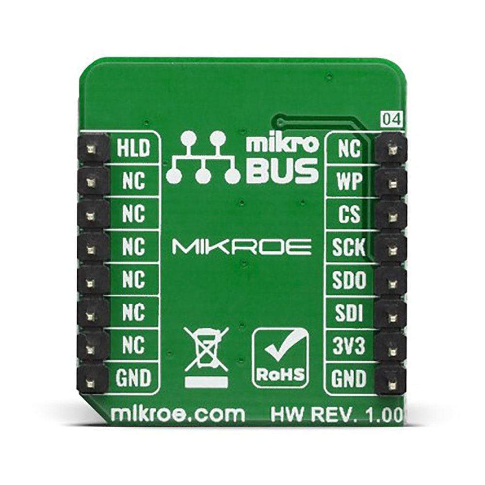
PINOUT DIAGRAM
This table shows how the pinout on the Flash 5 Click Board™ corresponds to the pinout on the mikroBUS™ socket (the latter shown in the two middle columns).
| Notes | Pin | Pin | Notes | ||||
|---|---|---|---|---|---|---|---|
| NC | 1 | AN | PWM | 16 | HLD | Hold | |
| Write Protect | WP | 2 | RST | INT | 15 | NC | |
| Chip Select | CS | 3 | CS | RX | 14 | NC | |
| SPI Clock | SCK | 4 | SCK | TX | 13 | NC | |
| SPI Data OUT/S01 | SDO | 5 | MISO | SCL | 12 | NC | |
| SPI Data IN/S00 | SDI | 6 | MOSI | SDA | 11 | NC | |
| Power Supply | 3.3V | 7 | 3.3V | 5V | 10 | NC | |
| Ground | GND | 8 | GND | GND | 9 | GND | Ground |
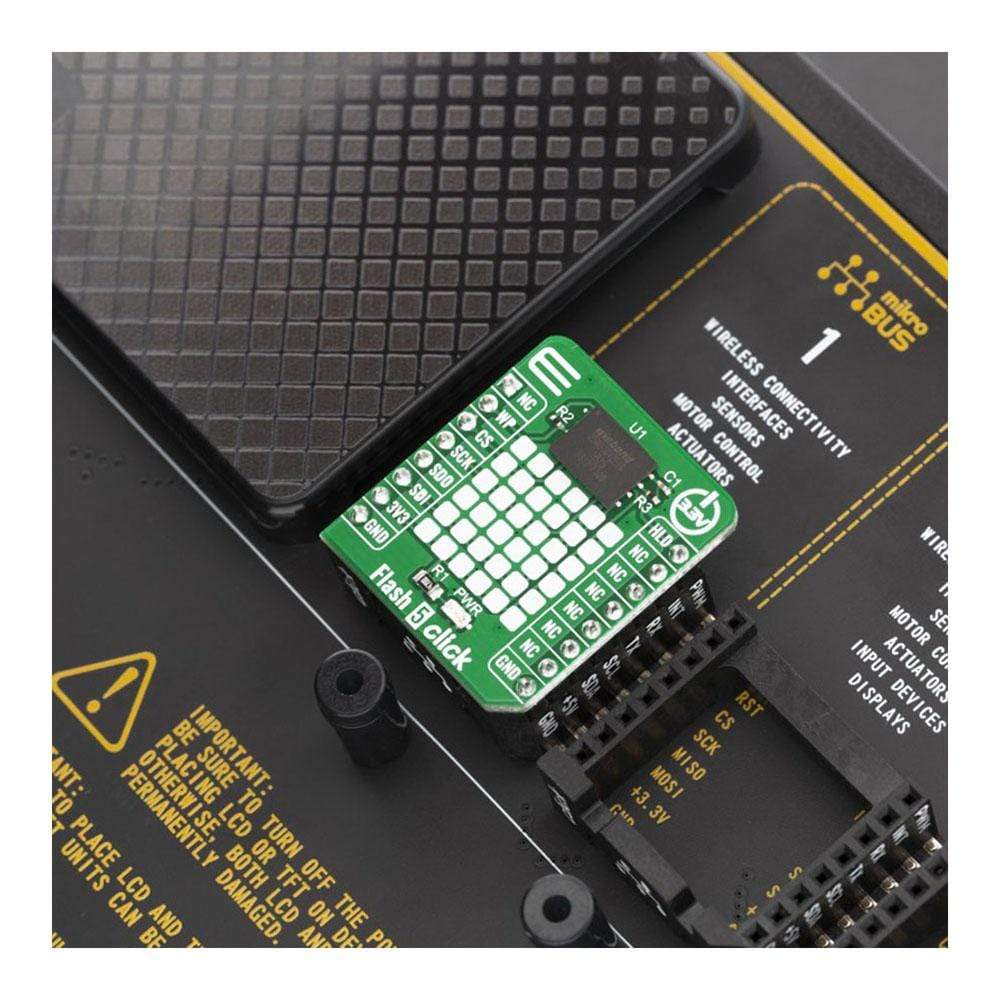
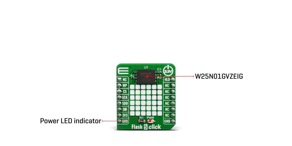
ONBOARD SETTINGS AND INDICATORS
| Label | Name | Default | Description |
|---|---|---|---|
| LD1 | PWR | - | Power LED Indicator |
| General Information | |
|---|---|
Part Number (SKU) |
MIKROE-3780
|
Manufacturer |
|
| Physical and Mechanical | |
Weight |
0.016 kg
|
| Other | |
EAN |
8606018719969
|
Frequently Asked Questions
Have a Question?
Be the first to ask a question about this.