


Mikroelektronika d.o.o.
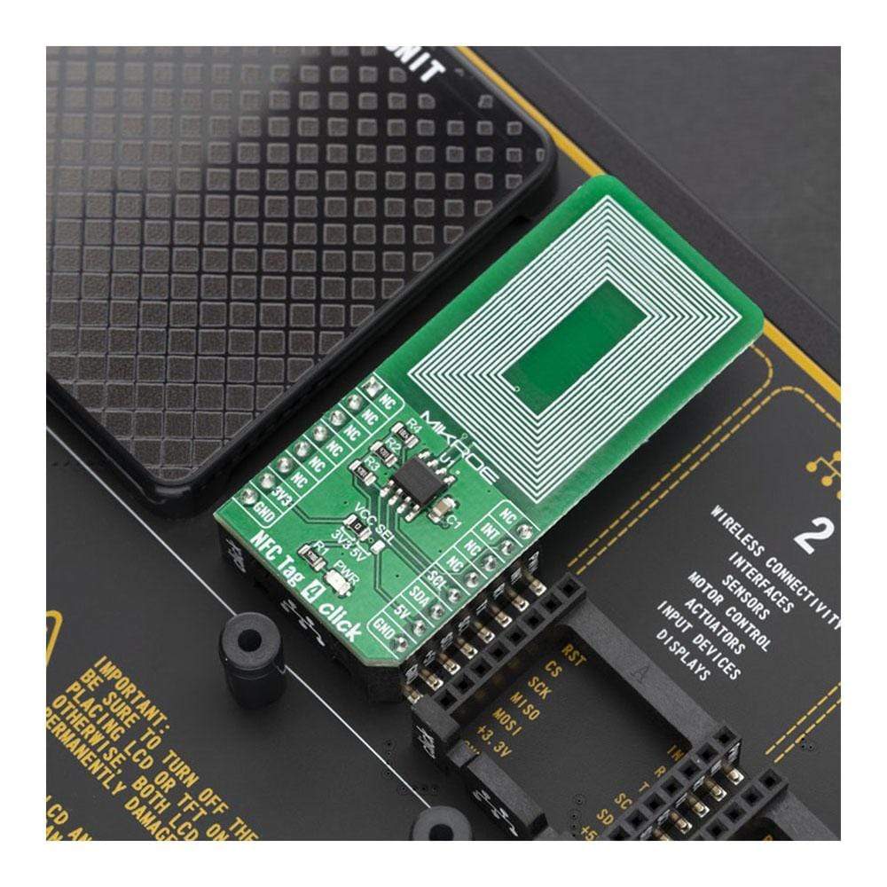
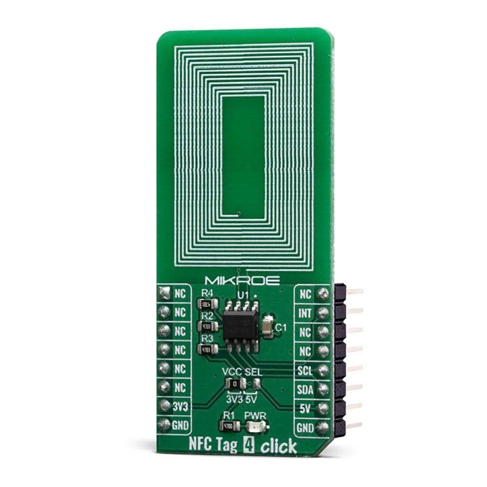
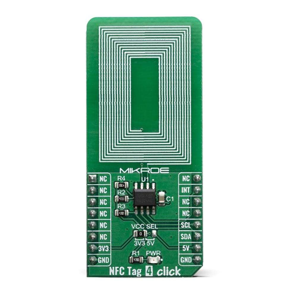
NFC Tag 4 Click Board™
NFC Tag 4 Click Board™
SKU: MIKROE-3659
Couldn't load pickup availability

Overview
The NFC Tag 4 Click Board™ is NFC tag device, offering 16 Kbit of electrically erasable programmable memory (EEPROM). This Click Board™ offers two communication interfaces. The first one is an I2C serial link and can be operated from a DC power supply. The second one is a RF link activated when Click Board™ act as a contactless memory powered by the received carrier electromagnetic wave. It is perfectly suited for using in wide variety of applications, such as NFC enabled business cards, stickers, wristbands, key fobs, pens, movie passes, hang tags, medication bottles, and many more.
The NFC Tag 4 Click Board™ is supported by a mikroSDK compliant library, which includes functions that simplify software development. This Click Board™ comes as a fully tested product, ready to be used on a system equipped with the mikroBUS™ socket.
Downloads
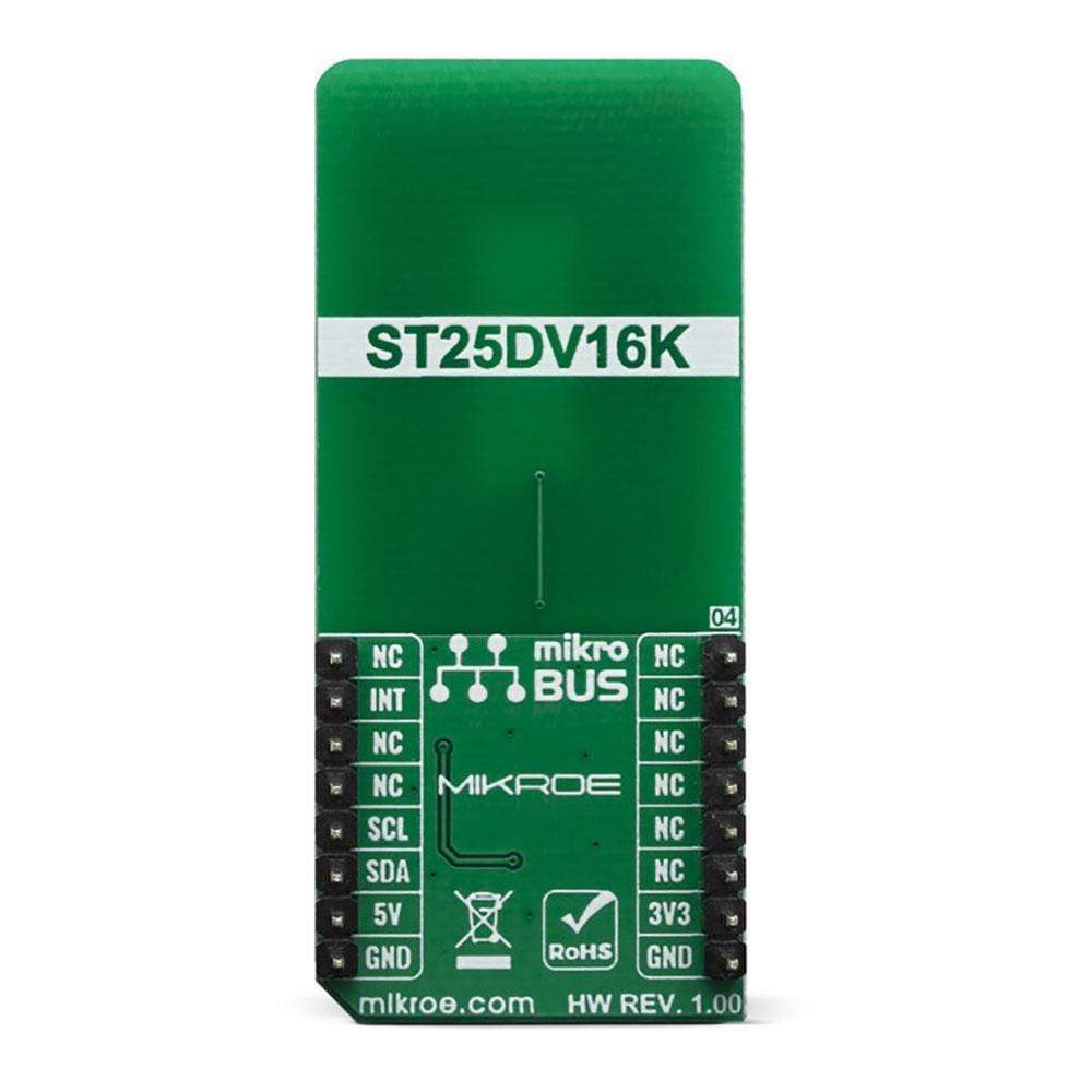
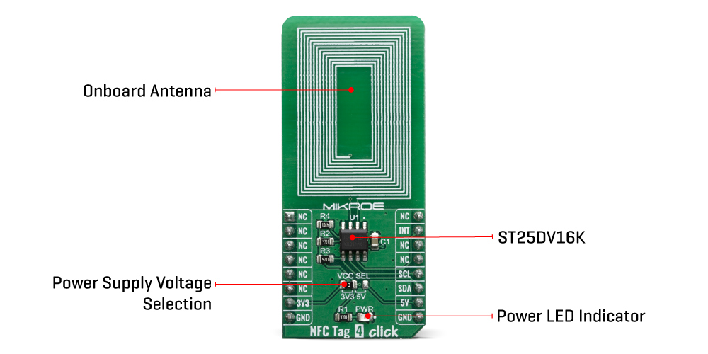
The NFC Tag 4 Click Board™ is NFC tag device, featuring ST25DV16K - the compact NFC tag IC from STMicroelectronics. This IC includes a full set of features, like Fast data transfer between I2C and RF interfaces, half-duplex 256-byte dedicated buffer, energy harvesting, data protection features, and more. NFC Tag 4 click also features the onboard trace antenna, ensuring that no external components are required in order to use this Click Board™.
How Does The NFC Tag 4 Click Board™ Work?
The active NFC tag component of the NFC Tag 4 Click Board™ is the ST25DV16K - the compact NFC tag IC from STMicroelectronics. The Click board™ itself has a reasonably small number of components because most of the interface and EEPROM memory circuitry is already integrated on the ST25DV16K IC. The I2C / SMBus compatible serial interface lines, along with the GPO pin, which also works in the open drain configuration, are pulled up by the onboard resistors. The 2-Wire lines are routed to the respective I2C lines of the mikroBUS™ (SCK and SDA), while the GPO pin of the main IC is routed to the INT pin of the mikroBUS™
The ST25DV16K uses the I2C/SMBus compatible communication interface, offering a fast transfer mode (FTM), to achieve a fast link between RF and contact worlds, via a 256 byte buffer called Mailbox. This mailbox dynamic buffer of 256 byte can be filled or emptied via either RF or I2C.
There is also the INT pin available, which indicates incoming event to the contact side, like RF Field changes, RF activity in progress, RF writing completion or Mailbox message availability. The built in energy harvesting element can deliver µW of power when external conditions make it possible. The integrated RF management allows the NFC Tag 4 click to ignore RF requests.
All these features can be programmed by setting static and/or dynamic registers of the ST25DV16K. ST25DVxxx can be partially customized using configuration registers located in the E2 system area. More information about all the registers can be found in the ST25DV16K datasheet. However, provided library contains functions that simplify the use of the NFC Tag 4 Click Board™. The included application example demonstrates their functionality and it can be used as a reference for custom design.
In order to make sure that no external components are required in order to use it, this Click Board™ contains the integrated trace antenna on the PCB. The antenna coil is correctly tuned and can be used to power and access the device using the ISO/IEC 15693 and ISO 18000-3 mode 1 protocols. Power is transferred to the ST25DV16K by radio frequency at 13.56 MHz via coupling antennas of the NFC Tag 4 click and the NFC Reader being used. The ISO 15693 standard defines the carrier frequency (fC) of the operating field as 13.56 MHz ±7 kHz.
The NFC Tag 4 Click Board™ can be supplied and interfaced with both 3.3V and 5V without the need for any external components. The onboard SMD jumper labelled as VCC SEL allows voltage selection for interfacing with both 3.3V and 5V MCUs.
SPECIFICATIONS
| Type | RFID/NFC |
| Applications | NFC enabled business cards, stickers, wristbands, key fobs, pens, movie passes, hang tags, medication bottles, and many more. |
| On-board modules | ST25DV16K - the compact NFC tag IC from STMicroelectronics |
| Key Features | Fast data transfer between I2C and RF interfaces, half-duplex 256-byte dedicated buffer, energy harvesting, data protection features, integrated antenna onboard |
| Interface | I2C |
| Compatibility | mikroBUS |
| Click board size | L (57.15 x 25.4 mm) |
| Input Voltage | 3.3V or 5V |
PINOUT DIAGRAM
This table shows how the pinout of the NFC Tag 4 Click Board™ corresponds to the pinout on the mikroBUS™ socket (the latter shown in the two middle columns).
| Notes | Pin | Pin | Notes | ||||
|---|---|---|---|---|---|---|---|
| NC | 1 | AN | PWM | 16 | NC | ||
| NC | 2 | RST | INT | 15 | INT | Interrupt output | |
| NC | 3 | CS | RX | 14 | NC | ||
| NC | 4 | SCK | TX | 13 | NC | ||
| NC | 5 | MISO | SCL | 12 | SCL | I2C Clock | |
| NC | 6 | MOSI | SDA | 11 | SDA | I2C Data | |
| Power Supply | 3.3V | 7 | 3.3V | 5V | 10 | 5V | Power Supply |
| Ground | GND | 8 | GND | GND | 9 | GND | Ground |
ONBOARD SETTINGS AND INDICATORS
| Label | Name | Default | Description |
|---|---|---|---|
| JP1 | VCC SEL | Left | Power supply voltage selection: left position 3V3, right position 5V |
| LD1 | PWR | - | Power LED indicator |
| General Information | |
|---|---|
Part Number (SKU) |
MIKROE-3659
|
Manufacturer |
|
| Physical and Mechanical | |
Weight |
0.019 kg
|
| Other | |
EAN |
8606018716425
|
Frequently Asked Questions
Have a Question?
Be the first to ask a question about this.